Voir les spécifications pour les détails du produit.

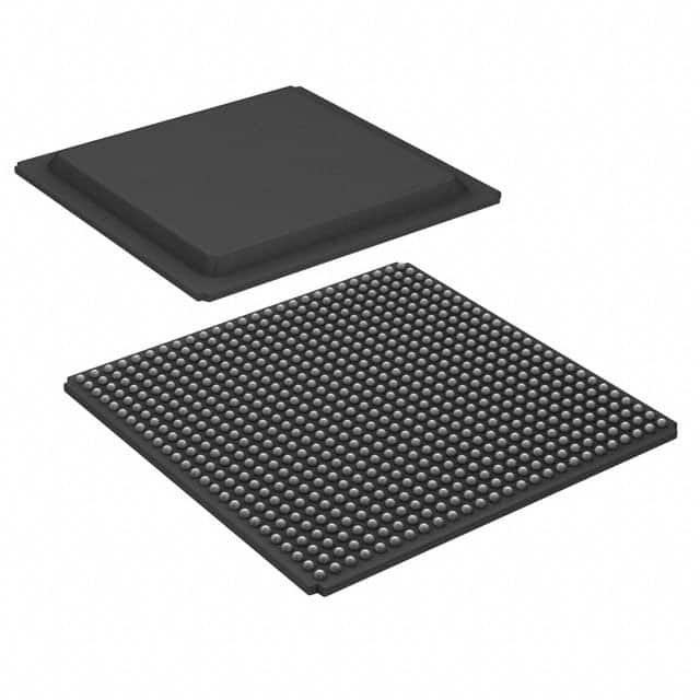
XCKU035-1FBVA676I
Product Overview
Category: Integrated Circuit (IC)
Use: XCKU035-1FBVA676I is a high-performance field-programmable gate array (FPGA) designed for various applications in the electronics industry.
Characteristics: - High-speed processing capabilities - Programmable logic cells - Flexible I/O interfaces - Large on-chip memory - Low power consumption
Package: The XCKU035-1FBVA676I is available in a 676-pin Ball Grid Array (BGA) package.
Essence: This FPGA offers a versatile and customizable solution for implementing complex digital circuits and systems.
Packaging/Quantity: The XCKU035-1FBVA676I is typically sold individually or in reels, with specific quantities depending on the supplier.
Specifications
- Logic Cells: 35,000
- DSP Slices: 560
- Block RAM: 2,520 Kb
- Clock Management Tiles: 16
- Transceivers: 32
- Operating Voltage: 1.0V
- Operating Temperature: -40°C to +100°C
Pin Configuration
The XCKU035-1FBVA676I has a detailed pin configuration with multiple I/O banks, power supply pins, and configuration pins. Please refer to the datasheet or user manual for the complete pinout information.
Functional Features
High-Speed Processing: The XCKU035-1FBVA676I offers fast data processing capabilities, making it suitable for applications requiring real-time performance.
Programmable Logic Cells: With 35,000 logic cells, this FPGA provides flexibility in designing complex digital circuits and implementing custom functionalities.
Flexible I/O Interfaces: The device supports various I/O standards, enabling seamless integration with different external devices and communication protocols.
Large On-Chip Memory: The generous on-chip memory capacity of 2,520 Kb allows for efficient data storage and retrieval within the FPGA itself.
Low Power Consumption: The XCKU035-1FBVA676I is designed to minimize power consumption, making it suitable for battery-powered or energy-efficient applications.
Advantages
- Versatile and customizable solution for digital circuit implementation
- High-speed processing capabilities enable real-time performance
- Flexible I/O interfaces for seamless integration with external devices
- Large on-chip memory reduces the need for external memory components
- Low power consumption for energy-efficient designs
Disadvantages
- Relatively high cost compared to other programmable logic devices
- Steep learning curve for beginners due to its complexity
- Limited availability of alternative models with similar specifications
Working Principles
The XCKU035-1FBVA676I operates based on the principles of field-programmable gate arrays. It consists of a large number of configurable logic cells interconnected through programmable routing resources. These logic cells can be programmed to implement various digital functions and algorithms. The device's functionality is determined by the configuration data loaded into it during initialization.
Application Field Plans
The XCKU035-1FBVA676I finds applications in various fields, including but not limited to: - Telecommunications - Aerospace and defense - Industrial automation - Medical equipment - Data processing and analytics
Its versatility and high-performance characteristics make it suitable for demanding applications that require complex digital processing and real-time performance.
Alternative Models
While the XCKU035-1FBVA676I offers unique features and specifications, there are alternative FPGA models available from different manufacturers. Some alternatives to consider include: - Xilinx Virtex UltraScale+ series - Intel (formerly Altera) Stratix 10 series - Lattice Semiconductor ECP5 series
These alternative models provide similar capabilities and can be evaluated based on specific project requirements and cost considerations.
Word count: 536 words
Énumérez 10 questions et réponses courantes liées à l'application de XCKU035-1FBVA676I dans les solutions techniques
Sure! Here are 10 common questions and answers related to the application of XCKU035-1FBVA676I in technical solutions:
Q1: What is the XCKU035-1FBVA676I? A1: The XCKU035-1FBVA676I is a field-programmable gate array (FPGA) device manufactured by Xilinx. It belongs to the Kintex UltraScale+ family and has 35,200 logic cells.
Q2: What are the key features of the XCKU035-1FBVA676I? A2: The key features of this FPGA include high-performance processing capabilities, advanced DSP functionality, integrated memory resources, multiple high-speed transceivers, and support for various communication protocols.
Q3: What are some typical applications of the XCKU035-1FBVA676I? A3: This FPGA is commonly used in applications such as wireless communication systems, aerospace and defense, industrial automation, video processing, high-performance computing, and scientific research.
Q4: What programming languages can be used with the XCKU035-1FBVA676I? A4: The XCKU035-1FBVA676I can be programmed using hardware description languages (HDLs) such as VHDL or Verilog. Xilinx's Vivado Design Suite is typically used for development and synthesis.
Q5: How many I/O pins does the XCKU035-1FBVA676I have? A5: This FPGA has a total of 676 I/O pins, which can be used for interfacing with external devices and peripherals.
Q6: What is the maximum clock frequency supported by the XCKU035-1FBVA676I? A6: The maximum clock frequency supported by this FPGA depends on the specific design and implementation. However, it is capable of operating at high speeds, typically in the range of several hundred megahertz to a few gigahertz.
Q7: Can the XCKU035-1FBVA676I be used for real-time signal processing? A7: Yes, this FPGA is well-suited for real-time signal processing applications due to its high-performance processing capabilities and integrated DSP functionality.
Q8: Does the XCKU035-1FBVA676I support high-speed serial communication? A8: Yes, this FPGA includes multiple high-speed transceivers that support various communication protocols such as PCIe, Ethernet, USB, and SATA.
Q9: What are the power requirements for the XCKU035-1FBVA676I? A9: The power requirements for this FPGA depend on the specific design and implementation. It typically operates at a voltage of 0.95V and requires multiple power supply rails.
Q10: Are there any development boards or evaluation kits available for the XCKU035-1FBVA676I? A10: Yes, Xilinx offers development boards and evaluation kits specifically designed for the XCKU035-1FBVA676I. These kits provide a platform for prototyping and testing designs using this FPGA.
Please note that the answers provided here are general and may vary depending on the specific requirements and implementation of the technical solution.

