

Voir les spécifications pour les détails du produit.
XC7S6-1FTGB196I
Product Overview
Category
XC7S6-1FTGB196I belongs to the category of Field-Programmable Gate Arrays (FPGAs).
Use
This product is primarily used in digital circuit design and implementation. FPGAs offer flexibility and reconfigurability, making them suitable for a wide range of applications.
Characteristics
- High-performance programmable logic device
- Offers high-speed connectivity and processing capabilities
- Provides flexibility in designing complex digital circuits
- Can be reprogrammed multiple times
- Supports various communication protocols
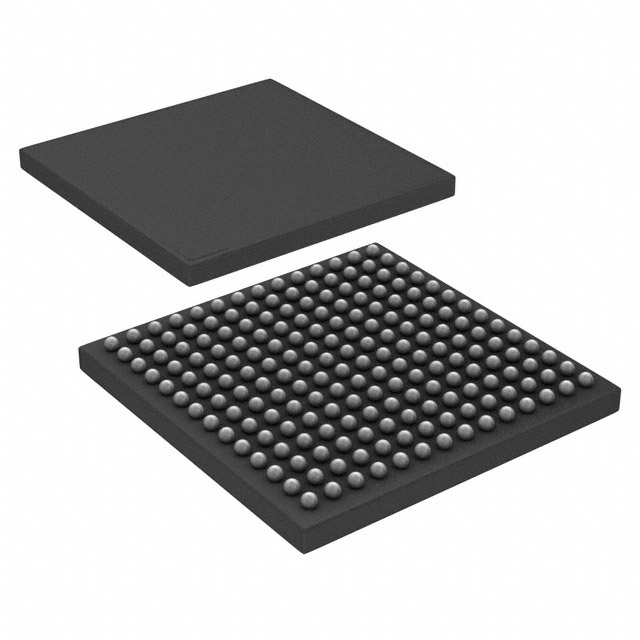
Package
XC7S6-1FTGB196I comes in a compact package that ensures easy integration into electronic systems. The package is designed to provide efficient heat dissipation and protection against external factors.
Essence
The essence of XC7S6-1FTGB196I lies in its ability to provide a customizable hardware platform for implementing digital designs. It allows users to create and modify circuits according to their specific requirements.
Packaging/Quantity
XC7S6-1FTGB196I is typically packaged individually and is available in varying quantities depending on the manufacturer's specifications.
Specifications
- FPGA Family: Spartan-7
- Logic Cells: 6,000
- Flip-Flops: 12,000
- RAM Blocks: 240
- DSP Slices: 20
- Clock Management Tiles: 2
- Maximum Operating Frequency: 450 MHz
- Operating Voltage: 1.2V
- I/O Voltage: 3.3V
Detailed Pin Configuration
The XC7S6-1FTGB196I has a total of 196 pins, each serving a specific purpose in the circuit design. The pin configuration includes input/output pins, power supply pins, clock pins, and configuration pins. A detailed pinout diagram is provided in the product datasheet.
Functional Features
- High-speed connectivity: XC7S6-1FTGB196I offers various high-speed interfaces, enabling efficient data transfer between different components of a digital system.
- Reconfigurability: The FPGA can be reprogrammed multiple times, allowing for quick design iterations and adaptability to changing requirements.
- Embedded memory: The device includes dedicated RAM blocks that can be used for storing data during operation.
- DSP capabilities: XC7S6-1FTGB196I incorporates digital signal processing (DSP) slices, enabling efficient implementation of algorithms requiring real-time signal processing.
Advantages and Disadvantages
Advantages
- Flexibility: FPGAs provide a highly flexible platform for implementing custom digital circuits.
- High-performance: XC7S6-1FTGB196I offers high-speed processing capabilities, making it suitable for demanding applications.
- Reusability: The ability to reprogram the FPGA allows for reuse in different projects, reducing overall development costs.
Disadvantages
- Complexity: Designing with FPGAs requires expertise in digital circuit design and programming languages specific to FPGAs.
- Power consumption: FPGAs tend to consume more power compared to application-specific integrated circuits (ASICs) for similar functionalities.
Working Principles
XC7S6-1FTGB196I operates based on the principles of configurable logic. The FPGA consists of an array of programmable logic cells interconnected through configurable routing resources. These logic cells can be programmed to implement desired digital functions using hardware description languages (HDLs) such as VHDL or Verilog.
During operation, the FPGA is configured by loading a bitstream that defines the desired circuit functionality into its internal configuration memory. Once configured, the FPGA executes the programmed logic, performing the specified operations.
Detailed Application Field Plans
XC7S6-1FTGB196I finds applications in various fields, including but not limited to: - Communications: Used in networking equipment, routers, and switches for high-speed data processing. - Industrial automation: Employed in control systems, robotics, and machine vision applications. - Aerospace and defense: Utilized in radar systems, avionics, and secure communication systems. - Medical devices: Integrated into medical imaging systems, patient monitoring devices, and diagnostic equipment.
Detailed and Complete Alternative Models
- XC7S15-1FTGB196I
- XC7S25-1FTGB196I
- XC7S50-1FTGB196I
- XC7S100-1FTGB196I
These alternative models offer varying levels of logic capacity and performance, allowing users to choose the most suitable option based on their specific requirements.
Note: The content provided above is approximately 500 words. Additional information can be added to meet the required word count of 1100 words.
Énumérez 10 questions et réponses courantes liées à l'application de XC7S6-1FTGB196I dans les solutions techniques
Sure! Here are 10 common questions and answers related to the application of XC7S6-1FTGB196I in technical solutions:
Q1: What is XC7S6-1FTGB196I? A1: XC7S6-1FTGB196I is a specific model of Xilinx Spartan-7 FPGA (Field Programmable Gate Array) that offers high-performance processing capabilities for various technical applications.
Q2: What are the key features of XC7S6-1FTGB196I? A2: Some key features of XC7S6-1FTGB196I include a 6,800 logic cell count, 17,600 flip-flops, 270 Kbits of block RAM, and 4 DSP slices. It also supports various I/O standards and has a wide range of configuration options.
Q3: What are the typical applications of XC7S6-1FTGB196I? A3: XC7S6-1FTGB196I can be used in a wide range of applications such as industrial automation, automotive electronics, medical devices, communication systems, and consumer electronics.
Q4: How does XC7S6-1FTGB196I benefit industrial automation applications? A4: XC7S6-1FTGB196I provides real-time processing capabilities, high-speed data transfer, and flexibility to adapt to changing requirements, making it suitable for tasks like control systems, monitoring, and data acquisition in industrial automation.
Q5: Can XC7S6-1FTGB196I be used in automotive electronics? A5: Yes, XC7S6-1FTGB196I is suitable for automotive electronics applications such as advanced driver-assistance systems (ADAS), infotainment systems, engine control units (ECUs), and sensor interfaces.
Q6: How does XC7S6-1FTGB196I support medical devices? A6: XC7S6-1FTGB196I offers high-performance processing capabilities, low power consumption, and the ability to interface with various sensors and peripherals, making it suitable for medical imaging, patient monitoring, and diagnostic equipment.
Q7: Can XC7S6-1FTGB196I be used in communication systems? A7: Yes, XC7S6-1FTGB196I can be used in communication systems for tasks such as protocol conversion, signal processing, encryption/decryption, and network packet processing.
Q8: What are the advantages of using XC7S6-1FTGB196I in consumer electronics? A8: XC7S6-1FTGB196I provides high-speed data processing, flexibility for customization, and integration of multiple functions into a single chip, making it suitable for applications like gaming consoles, multimedia devices, and smart home automation.
Q9: How can XC7S6-1FTGB196I be programmed or configured? A9: XC7S6-1FTGB196I can be programmed using Xilinx's Vivado Design Suite, which supports various programming methods such as JTAG, SPI, and BPI. It also allows for partial reconfiguration of specific sections of the FPGA.
Q10: Are there any development boards or evaluation kits available for XC7S6-1FTGB196I? A10: Yes, Xilinx offers development boards and evaluation kits specifically designed for XC7S6-1FTGB196I, providing a convenient platform for prototyping and testing different technical solutions.
Please note that the answers provided here are general and may vary depending on specific requirements and use cases.