

Voir les spécifications pour les détails du produit.
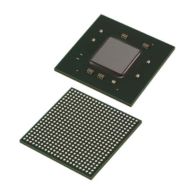
XC7K160T-2FB484I
Product Overview
Category
The XC7K160T-2FB484I belongs to the category of Field Programmable Gate Arrays (FPGAs).
Use
FPGAs are integrated circuits that can be programmed and reprogrammed to perform various digital functions. The XC7K160T-2FB484I is specifically designed for high-performance applications that require complex digital processing.
Characteristics
- High-performance FPGA with advanced features
- Large capacity and high-speed processing capabilities
- Flexible and reconfigurable design
- Suitable for a wide range of applications
Package
The XC7K160T-2FB484I comes in a compact and durable package, ensuring easy handling and protection against external factors such as moisture and static electricity.
Essence
The essence of the XC7K160T-2FB484I lies in its ability to provide a customizable and powerful digital processing solution for various applications.
Packaging/Quantity
The XC7K160T-2FB484I is typically packaged individually and is available in varying quantities depending on the customer's requirements.
Specifications
- FPGA Family: Kintex-7
- Device Type: XC7K160T
- Package Type: FB484
- Number of Logic Cells: 159,200
- Number of DSP Slices: 720
- Maximum Operating Frequency: 600 MHz
- Number of I/Os: 400
- Operating Voltage: 1.0V
Detailed Pin Configuration
The XC7K160T-2FB484I has a total of 400 I/O pins, each serving a specific purpose in the overall functionality of the FPGA. For detailed pin configuration information, please refer to the manufacturer's datasheet.
Functional Features
- High-performance digital signal processing capabilities
- Configurable logic blocks for custom circuit implementation
- Integrated memory blocks for efficient data storage and retrieval
- Flexible I/O interfaces for seamless integration with external devices
- Advanced clock management resources for precise timing control
Advantages and Disadvantages
Advantages
- High processing power and performance
- Flexibility to adapt to changing requirements
- Reconfigurable design allows for iterative development
- Wide range of available resources and libraries
- Support for various programming languages and tools
Disadvantages
- Steep learning curve for beginners
- Higher cost compared to other digital processing solutions
- Requires specialized knowledge for optimal utilization
- Limited availability of technical support for complex issues
Working Principles
The XC7K160T-2FB484I operates based on the principles of reconfigurable logic. It consists of a matrix of configurable logic blocks interconnected through programmable routing resources. The FPGA can be programmed using Hardware Description Languages (HDLs) such as VHDL or Verilog, which define the desired functionality of the circuit. Once programmed, the FPGA executes the specified operations by routing signals through the configured logic blocks.
Detailed Application Field Plans
The XC7K160T-2FB484I finds applications in various fields that require high-performance digital processing capabilities. Some potential application areas include:
- Telecommunications: Signal processing, encryption/decryption, and protocol handling.
- Aerospace and Defense: Radar systems, image processing, and communication systems.
- Industrial Automation: Control systems, machine vision, and robotics.
- Medical Imaging: Image reconstruction, signal analysis, and real-time processing.
- High-Frequency Trading: Algorithmic trading, market data analysis, and latency-sensitive operations.
Detailed and Complete Alternative Models
- XC7A200T-2FBG676C: A similar FPGA from the same family with higher logic capacity and more I/O pins.
- XC7Z045-2FFG900I: A hybrid FPGA with integrated ARM processor for embedded system applications.
- XC6SLX150T-2FGG484C: An alternative FPGA from a different family, offering a balance between cost and performance.
These alternative models provide varying capabilities and features to cater to different application requirements.
Word count: 550 words
Énumérez 10 questions et réponses courantes liées à l'application de XC7K160T-2FB484I dans les solutions techniques
Sure! Here are 10 common questions and answers related to the application of XC7K160T-2FB484I in technical solutions:
Q: What is XC7K160T-2FB484I? A: XC7K160T-2FB484I is a specific model of Xilinx's Kintex-7 FPGA family, which offers high-performance programmable logic for various technical applications.
Q: What are the key features of XC7K160T-2FB484I? A: Some key features include 160,000 logic cells, 4-input look-up tables, high-speed serial transceivers, integrated memory controllers, and DSP slices.
Q: What are the typical applications of XC7K160T-2FB484I? A: XC7K160T-2FB484I is commonly used in applications such as wireless communication systems, video processing, industrial automation, medical imaging, and aerospace systems.
Q: How can I program XC7K160T-2FB484I? A: XC7K160T-2FB484I can be programmed using Xilinx's Vivado Design Suite, which provides a comprehensive development environment for FPGA designs.
Q: Can XC7K160T-2FB484I be used for real-time signal processing? A: Yes, XC7K160T-2FB484I is well-suited for real-time signal processing due to its high-performance capabilities and integrated DSP slices.
Q: Does XC7K160T-2FB484I support high-speed serial communication protocols? A: Yes, XC7K160T-2FB484I includes multiple high-speed serial transceivers that support protocols like PCIe, SATA, USB, and Ethernet.
Q: Can XC7K160T-2FB484I interface with external memory devices? A: Yes, XC7K160T-2FB484I has integrated memory controllers that support various memory interfaces like DDR3, DDR4, and QDR.
Q: What is the power consumption of XC7K160T-2FB484I? A: The power consumption of XC7K160T-2FB484I depends on the specific design and operating conditions but typically ranges from a few watts to tens of watts.
Q: Are there any development boards available for XC7K160T-2FB484I? A: Yes, Xilinx offers development boards like the Kintex-7 KC705 Evaluation Kit, which provide a platform for prototyping and testing designs using XC7K160T-2FB484I.
Q: Where can I find more information about XC7K160T-2FB484I? A: You can find detailed technical documentation, datasheets, and application notes on Xilinx's official website or by referring to the product documentation provided by Xilinx.