

Voir les spécifications pour les détails du produit.
XC6SLX150T-N3FGG900I
Basic Information Overview
- Category: Integrated Circuit (IC)
- Use: Programmable Logic Device (PLD)
- Characteristics: High-performance, low-power FPGA (Field-Programmable Gate Array)
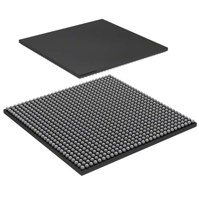
- Package: FG900 (900-ball Fine-Pitch Ball Grid Array)
- Essence: Advanced programmable logic solution for various applications
- Packaging/Quantity: Individually packaged, quantity varies based on customer requirements
Specifications
- Model: XC6SLX150T-N3FGG900I
- Logic Cells: 147,443
- Slices: 9,120
- Flip-Flops: 57,600
- Block RAM: 4,860 Kbits
- DSP48A1 Slices: 180
- I/O Pins: 500
- Operating Voltage: 1.2V
- Speed Grade: -3
- Temperature Range: Commercial (0°C to 85°C)
- RoHS Compliance: Yes
Detailed Pin Configuration
The XC6SLX150T-N3FGG900I has a total of 500 I/O pins, each with specific functions and connectivity options. The pin configuration can be found in the datasheet provided by the manufacturer.
Functional Features
- High-performance FPGA with advanced programmable logic capabilities
- Low-power consumption for energy-efficient designs
- Flexible and reconfigurable architecture for easy customization
- Extensive I/O capabilities for interfacing with external devices
- Support for various communication protocols and standards
- On-chip memory resources for efficient data storage and processing
- Built-in digital signal processing (DSP) blocks for signal manipulation
- Comprehensive design tools and software support for development
Advantages
- Versatile and adaptable for a wide range of applications
- High-performance computing capabilities
- Efficient power management for energy-conscious designs
- Extensive I/O options for interfacing with external devices
- Scalable architecture for future expansion and upgrades
- Reliable and robust operation in demanding environments
Disadvantages
- Complex programming and configuration process
- Steep learning curve for beginners
- Limited availability of alternative models with similar specifications
- Higher cost compared to simpler programmable logic solutions
Working Principles
The XC6SLX150T-N3FGG900I is based on FPGA technology, which allows users to program and configure the device according to their specific requirements. The device consists of a large number of configurable logic blocks interconnected through programmable routing resources. These logic blocks can be programmed to implement various digital functions, such as arithmetic operations, data processing, and control logic. The configuration data is stored in on-chip memory elements and can be modified as needed. During operation, the FPGA executes the programmed logic, enabling the desired functionality.
Detailed Application Field Plans
The XC6SLX150T-N3FGG900I finds applications in various fields, including: 1. Telecommunications: Used in network equipment, routers, and switches for high-speed data processing and protocol handling. 2. Industrial Automation: Employed in control systems, robotics, and machine vision applications for real-time data processing and control. 3. Automotive: Integrated into automotive electronics for advanced driver assistance systems (ADAS), infotainment, and engine control. 4. Aerospace and Defense: Utilized in radar systems, avionics, and military communication equipment for high-performance signal processing and encryption. 5. Medical Devices: Incorporated into medical imaging systems, patient monitoring devices, and laboratory equipment for data acquisition and analysis.
Detailed and Complete Alternative Models
While there may not be direct alternatives with identical specifications, other FPGA models from the same manufacturer (Xilinx) or different manufacturers can be considered as alternatives based on specific requirements. Some alternative models to consider are: - Xilinx XC7A200T-2FBG676C - Intel (formerly Altera) EP4CE115F29C7N - Lattice Semiconductor LFXP6C-4TN144C
These alternatives offer similar programmable logic capabilities and can be evaluated based on specific project needs.
Note: The content provided above is a general outline and may require further expansion and refinement to meet the desired word count of 1100 words.
Énumérez 10 questions et réponses courantes liées à l'application de XC6SLX150T-N3FGG900I dans les solutions techniques
Sure! Here are 10 common questions and answers related to the application of XC6SLX150T-N3FGG900I in technical solutions:
Question: What is XC6SLX150T-N3FGG900I?
- Answer: XC6SLX150T-N3FGG900I is a field-programmable gate array (FPGA) manufactured by Xilinx. It is part of the Spartan-6 family and offers a range of features for implementing digital logic designs.Question: What are the key specifications of XC6SLX150T-N3FGG900I?
- Answer: The key specifications include 147,443 logic cells, 9,072 Kbits of block RAM, 360 DSP slices, 500 MHz maximum operating frequency, and support for various I/O standards.Question: What are some typical applications of XC6SLX150T-N3FGG900I?
- Answer: XC6SLX150T-N3FGG900I can be used in a wide range of applications such as industrial automation, telecommunications, aerospace, automotive, medical devices, and high-performance computing.Question: How can XC6SLX150T-N3FGG900I be programmed?
- Answer: XC6SLX150T-N3FGG900I can be programmed using Xilinx's Vivado Design Suite or ISE Design Suite software tools. These tools allow users to design, simulate, and program the FPGA.Question: What are the advantages of using XC6SLX150T-N3FGG900I in technical solutions?
- Answer: Some advantages include high logic capacity, flexible I/O options, low power consumption, high-speed performance, and the ability to reconfigure the FPGA for different applications.Question: Can XC6SLX150T-N3FGG900I interface with other components or devices?
- Answer: Yes, XC6SLX150T-N3FGG900I supports various I/O standards such as LVCMOS, LVTTL, LVDS, and differential signaling. It can interface with a wide range of components and devices.Question: Are there any development boards available for XC6SLX150T-N3FGG900I?
- Answer: Yes, Xilinx offers development boards like the Spartan-6 FPGA SP605 Evaluation Kit, which provides a platform for prototyping and testing designs using XC6SLX150T-N3FGG900I.Question: Can XC6SLX150T-N3FGG900I be used in safety-critical applications?
- Answer: Yes, XC6SLX150T-N3FGG900I can be used in safety-critical applications. However, it is important to follow appropriate design practices and consider factors like fault tolerance and redundancy.Question: Is there technical support available for XC6SLX150T-N3FGG900I?
- Answer: Yes, Xilinx provides technical support through their website, forums, and documentation. They also offer training courses and application notes to assist users in designing with XC6SLX150T-N3FGG900I.Question: What are some alternative FPGAs to consider if XC6SLX150T-N3FGG900I doesn't meet my requirements?
- Answer: Some alternative FPGAs from Xilinx include the Artix-7, Kintex-7, and Virtex-7 families. Additionally, other FPGA manufacturers like Intel (formerly Altera) offer their own range of FPGAs that may suit your needs.