Voir les spécifications pour les détails du produit.

XC6SLX100-3FGG484I
Product Overview
Category
XC6SLX100-3FGG484I belongs to the category of Field Programmable Gate Arrays (FPGAs).
Use
This product is widely used in various electronic applications that require high-performance digital signal processing, such as telecommunications, automotive, aerospace, and industrial control systems.
Characteristics
- High-speed performance: The XC6SLX100-3FGG484I offers fast processing capabilities, making it suitable for real-time applications.
- Programmability: It can be reprogrammed to implement different logic functions, allowing for flexibility in design.
- Low power consumption: This FPGA is designed to minimize power consumption, making it energy-efficient.
- Large capacity: With a capacity of 100,000 logic cells, it can handle complex designs and algorithms.
- Integrated features: The XC6SLX100-3FGG484I includes built-in memory blocks, DSP slices, and high-speed I/O interfaces.
Package and Quantity
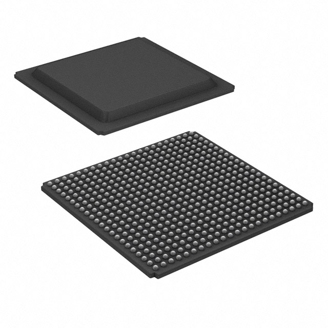
The XC6SLX100-3FGG484I comes in a FG484 package. Each package contains one unit of the FPGA.
Specifications
- Logic Cells: 100,000
- Block RAM: 4,860 Kbits
- DSP Slices: 240
- Maximum Frequency: 550 MHz
- I/O Pins: 484
- Operating Voltage: 1.2V
- Operating Temperature: -40°C to 100°C
Detailed Pin Configuration
The XC6SLX100-3FGG484I has a total of 484 I/O pins, each serving a specific purpose in the system. These pins are organized into banks and support various voltage standards, including LVCMOS, LVTTL, and SSTL.
For a detailed pin configuration diagram and description, please refer to the product datasheet.
Functional Features
- High-speed data processing: The XC6SLX100-3FGG484I offers fast data processing capabilities, enabling real-time applications.
- Flexible design: Its programmable nature allows for easy modification and adaptation to changing requirements.
- Integrated peripherals: The FPGA includes built-in memory blocks and DSP slices, reducing the need for external components.
- High-speed I/O interfaces: It supports various high-speed serial communication protocols, such as PCIe and Ethernet.
Advantages and Disadvantages
Advantages
- Versatility: The XC6SLX100-3FGG484I can be used in a wide range of applications due to its flexibility and high-performance capabilities.
- Energy-efficient: Its low power consumption makes it suitable for battery-powered devices.
- Integration: The FPGA's integrated features reduce the need for additional components, simplifying the overall system design.
Disadvantages
- Complexity: Working with FPGAs requires specialized knowledge and expertise, making it challenging for beginners.
- Cost: FPGAs can be more expensive compared to other programmable logic devices or microcontrollers.
- Limited analog capabilities: FPGAs primarily focus on digital signal processing and may have limited analog functionality.
Working Principles
The XC6SLX100-3FGG484I is based on the principle of reconfigurable logic. It consists of an array of configurable logic blocks (CLBs) interconnected through programmable routing resources. These CLBs can be programmed to implement various logic functions, allowing for custom designs.
The FPGA's configuration is stored in internal memory cells, which can be reprogrammed using specialized software tools. During operation, the FPGA executes the configured logic functions, processing input signals and generating output signals accordingly.
Detailed Application Field Plans
The XC6SLX100-3FGG484I finds extensive use in the following application fields:
- Telecommunications: It is employed in high-speed data transmission systems, network routers, and wireless communication devices.
- Automotive: The FPGA is utilized in automotive control systems, including engine management, advanced driver-assistance systems (ADAS), and infotainment systems.
- Aerospace: It plays a crucial role in avionics systems, satellite communication, and radar signal processing.
- Industrial Control Systems: The XC6SLX100-3FGG484I is used in industrial automation, robotics, and process control applications.
Detailed and Complete Alternative Models
- XC7A35T-1CPG236C
- XC7K160T-2FBG676I
- XC7Z020-1CLG400C
- XC7S50-1CSGA324C
- XC7VX690T-2FFG1761I
These alternative models offer similar functionality and performance characteristics to the XC6SLX100-3FGG484I. However, each model may have different capacity, pin configuration, or package options. It is recommended to refer to the respective
Énumérez 10 questions et réponses courantes liées à l'application de XC6SLX100-3FGG484I dans les solutions techniques
Sure! Here are 10 common questions and answers related to the application of XC6SLX100-3FGG484I in technical solutions:
Q: What is XC6SLX100-3FGG484I? A: XC6SLX100-3FGG484I is a field-programmable gate array (FPGA) manufactured by Xilinx. It belongs to the Spartan-6 family and has 100,000 logic cells.
Q: What are the key features of XC6SLX100-3FGG484I? A: Some key features include a high logic density, low power consumption, advanced DSP capabilities, integrated memory blocks, and support for various I/O standards.
Q: What applications can XC6SLX100-3FGG484I be used for? A: XC6SLX100-3FGG484I can be used in a wide range of applications such as industrial automation, telecommunications, automotive electronics, medical devices, aerospace, and defense systems.
Q: How can I program XC6SLX100-3FGG484I? A: XC6SLX100-3FGG484I can be programmed using Xilinx's Vivado Design Suite or ISE Design Suite software tools. These tools allow you to write and compile your design code and then program it onto the FPGA.
Q: What is the maximum operating frequency of XC6SLX100-3FGG484I? A: The maximum operating frequency of XC6SLX100-3FGG484I depends on the specific design and implementation. However, it can typically operate at frequencies up to several hundred megahertz.
Q: Can XC6SLX100-3FGG484I interface with other components or devices? A: Yes, XC6SLX100-3FGG484I supports various I/O standards such as LVCMOS, LVTTL, LVDS, and differential signaling. This allows it to interface with a wide range of components and devices.
Q: What is the power consumption of XC6SLX100-3FGG484I? A: The power consumption of XC6SLX100-3FGG484I depends on the specific design and utilization. However, it is designed to be power-efficient and offers low-power modes to conserve energy.
Q: Can XC6SLX100-3FGG484I be used for real-time signal processing? A: Yes, XC6SLX100-3FGG484I has advanced digital signal processing (DSP) capabilities, including dedicated DSP slices and multiply-accumulate (MAC) units, making it suitable for real-time signal processing applications.
Q: Does XC6SLX100-3FGG484I support partial reconfiguration? A: Yes, XC6SLX100-3FGG484I supports partial reconfiguration, allowing you to dynamically change a portion of the FPGA's configuration while the rest of the design remains operational.
Q: Are there any development boards or evaluation kits available for XC6SLX100-3FGG484I? A: Yes, Xilinx offers development boards and evaluation kits specifically designed for XC6SLX100-3FGG484I, such as the Spartan-6 FPGA SP605 Evaluation Kit, which provides a platform for prototyping and testing designs.

