Voir les spécifications pour les détails du produit.

XC6SLX100-3FG676C
Product Overview
Category
XC6SLX100-3FG676C belongs to the category of Field Programmable Gate Arrays (FPGAs).
Use
FPGAs are integrated circuits that can be programmed and reprogrammed to perform various digital functions. They are widely used in industries such as telecommunications, automotive, aerospace, and consumer electronics.
Characteristics
XC6SLX100-3FG676C is known for its high performance, low power consumption, and flexibility. It offers a large number of configurable logic blocks, on-chip memory, and high-speed I/O interfaces.
Package
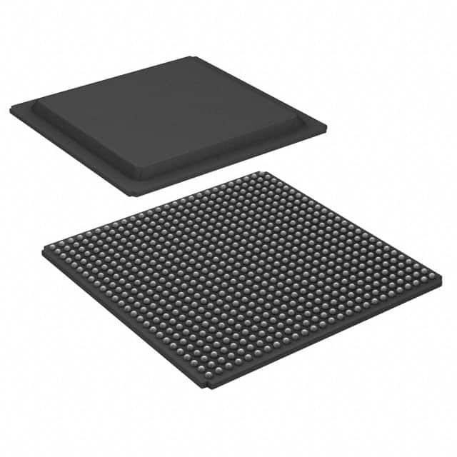
XC6SLX100-3FG676C comes in a FG676C package, which refers to a fine-pitch ball grid array (BGA) package with 676 solder balls.
Essence
The essence of XC6SLX100-3FG676C lies in its ability to provide a customizable hardware platform that allows designers to implement complex digital systems efficiently.
Packaging/Quantity
XC6SLX100-3FG676C is typically packaged in trays or reels, depending on the manufacturer's specifications. The quantity per package varies but is usually in the range of 10 to 100 units.
Specifications
- Logic Cells: 101,440
- Flip-Flops: 64,000
- Block RAM: 4,860 Kbits
- DSP Slices: 240
- Maximum Operating Frequency: 550 MHz
- I/O Pins: 500
- Voltage Range: 1.14V - 1.26V
Detailed Pin Configuration
XC6SLX100-3FG676C has a total of 676 pins arranged in a fine-pitch ball grid array (BGA) package. Each pin serves a specific purpose, including input, output, power, and ground connections. The pin configuration is detailed in the product datasheet provided by the manufacturer.
Functional Features
XC6SLX100-3FG676C offers several functional features that make it a versatile FPGA for various applications:
- Configurable Logic Blocks (CLBs): These blocks provide the building blocks for implementing digital logic functions within the FPGA.
- High-Speed I/O Interfaces: XC6SLX100-3FG676C supports a wide range of high-speed serial and parallel interfaces, enabling fast data transfer.
- On-Chip Memory: The FPGA includes embedded block RAMs that can be used for storing data or implementing memory-intensive functions.
- Digital Signal Processing (DSP) Slices: These dedicated hardware blocks enable efficient implementation of complex mathematical operations commonly found in signal processing applications.
Advantages and Disadvantages
Advantages
- High performance and flexibility due to its large number of logic cells and configurable resources.
- Low power consumption compared to traditional ASIC designs.
- Rapid prototyping and development cycles enabled by the reprogrammable nature of FPGAs.
- Ability to implement complex digital systems on a single chip.
Disadvantages
- Higher cost compared to fixed-function integrated circuits.
- Limited maximum operating frequency compared to dedicated application-specific chips.
- Design complexity increases with the size and scale of the FPGA.
Working Principles
XC6SLX100-3FG676C operates based on the principles of reconfigurable computing. It consists of an array of configurable logic blocks interconnected through programmable routing resources. The device can be programmed using Hardware Description Languages (HDLs) such as VHDL or Verilog, which describe the desired functionality of the digital system. Once programmed, the FPGA executes the specified logic functions, allowing for the implementation of custom digital circuits.
Detailed Application Field Plans
XC6SLX100-3FG676C finds applications in various fields, including:
- Telecommunications: Used in base stations, routers, and network switches for high-speed data processing and protocol handling.
- Automotive: Employed in advanced driver-assistance systems (ADAS), infotainment systems, and engine control units (ECUs) for real-time processing and control.
- Aerospace: Utilized in satellite communication systems, avionics, and radar systems for their high-performance computing capabilities.
- Consumer Electronics: Found in gaming consoles, high-definition televisions, and multimedia devices for video and audio processing.
Detailed and Complete Alternative Models
- XC6SLX150-3FG676C
- XC6SLX75-3FG676C
- XC6SLX25-3FG676C
- XC6SLX45-3FG676C
These alternative models offer different logic capacities and performance levels, allowing designers to choose the most suitable FPGA for their specific requirements.
In conclusion, XC6SLX100-3FG676C is a high-performance FPGA that provides flexibility, low power consumption, and a wide range of applications. Its configurable
Énumérez 10 questions et réponses courantes liées à l'application de XC6SLX100-3FG676C dans les solutions techniques
Sure! Here are 10 common questions and answers related to the application of XC6SLX100-3FG676C in technical solutions:
Q: What is XC6SLX100-3FG676C? A: XC6SLX100-3FG676C is a field-programmable gate array (FPGA) manufactured by Xilinx. It belongs to the Spartan-6 LX family and has 100,000 logic cells.
Q: What are the key features of XC6SLX100-3FG676C? A: Some key features of XC6SLX100-3FG676C include high-performance logic fabric, integrated memory blocks, DSP slices, clock management resources, and various I/O options.
Q: What applications can XC6SLX100-3FG676C be used for? A: XC6SLX100-3FG676C can be used in a wide range of applications such as industrial automation, telecommunications, automotive electronics, medical devices, aerospace, and defense systems.
Q: How does XC6SLX100-3FG676C differ from other FPGAs? A: XC6SLX100-3FG676C offers a good balance between cost, performance, and power consumption. It provides a large number of logic cells, memory blocks, and I/O options at an affordable price point.
Q: What development tools are available for programming XC6SLX100-3FG676C? A: Xilinx provides Vivado Design Suite, which includes tools like Vivado IDE, Vivado HLS, and Vivado SDK, to program and configure XC6SLX100-3FG676C.
Q: Can XC6SLX100-3FG676C be used for high-speed data processing? A: Yes, XC6SLX100-3FG676C supports high-speed serial transceivers and has dedicated DSP slices that can be used for efficient data processing and signal manipulation.
Q: How can I interface XC6SLX100-3FG676C with other components or devices? A: XC6SLX100-3FG676C provides a variety of I/O standards such as LVCMOS, LVTTL, LVDS, and differential signaling options, making it compatible with different interfaces and protocols.
Q: Can XC6SLX100-3FG676C be reprogrammed after deployment? A: Yes, XC6SLX100-3FG676C is a field-programmable device, which means it can be reprogrammed even after it has been deployed in a system.
Q: What are the power requirements for XC6SLX100-3FG676C? A: XC6SLX100-3FG676C typically operates at a voltage range of 1.14V to 1.26V, and its power consumption depends on the design and utilization of the FPGA resources.
Q: Are there any specific design considerations when using XC6SLX100-3FG676C? A: It is important to consider factors like clocking, power supply decoupling, thermal management, and proper board layout techniques to ensure optimal performance and reliability when using XC6SLX100-3FG676C.
Please note that these answers are general and may vary depending on specific requirements and design considerations.

