Voir les spécifications pour les détails du produit.

XC6SLX100-3FG484I
Product Overview
Category
The XC6SLX100-3FG484I belongs to the category of Field Programmable Gate Arrays (FPGAs).
Use
FPGAs are integrated circuits that can be programmed and reprogrammed to perform various digital functions. The XC6SLX100-3FG484I is specifically designed for high-performance applications.
Characteristics
- High-speed processing capabilities
- Configurable logic blocks
- On-chip memory
- Flexible I/O options
- Low power consumption
Package
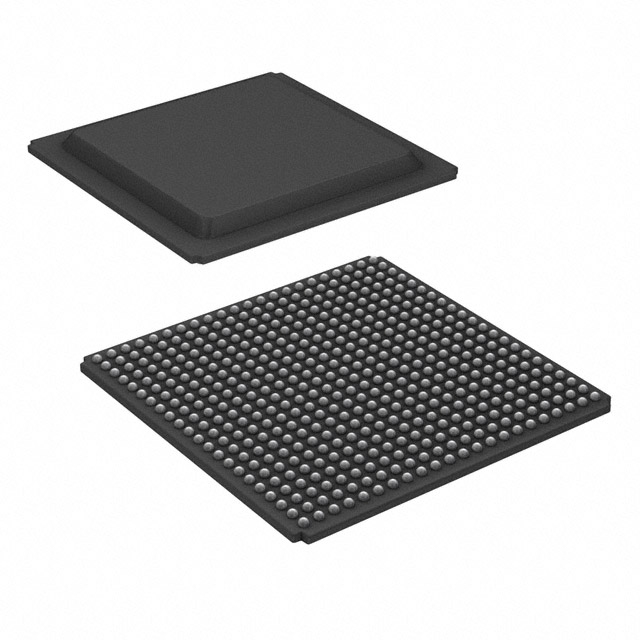
The XC6SLX100-3FG484I comes in a FG484 package, which refers to a fine-pitch ball grid array with 484 pins.
Essence
The essence of the XC6SLX100-3FG484I lies in its ability to provide customizable digital logic functions, allowing designers to implement complex systems on a single chip.
Packaging/Quantity
The XC6SLX100-3FG484I is typically packaged individually and is available in varying quantities depending on the manufacturer or distributor.
Specifications
- Logic Cells: 101,440
- Flip-Flops: 64,000
- Block RAM: 4,860 Kbits
- DSP Slices: 240
- Maximum Frequency: 550 MHz
- Operating Voltage: 1.2V
- Operating Temperature Range: -40°C to +100°C
Detailed Pin Configuration
The XC6SLX100-3FG484I has a total of 484 pins, each serving a specific purpose. The pin configuration includes input/output pins, power supply pins, ground pins, and configuration pins. A detailed pinout diagram can be found in the product datasheet.
Functional Features
- High-speed data processing
- Reconfigurability for design flexibility
- Support for various communication protocols
- On-chip memory for data storage
- Built-in digital signal processing capabilities
Advantages and Disadvantages
Advantages
- Versatility: Can be programmed to perform a wide range of functions.
- Flexibility: Allows for design modifications without the need for hardware changes.
- Integration: Combines multiple components into a single chip, reducing system complexity.
- Time-to-Market: Shorter development cycles compared to custom ASIC designs.
Disadvantages
- Power Consumption: FPGAs generally consume more power compared to dedicated application-specific integrated circuits (ASICs).
- Cost: FPGAs can be more expensive than off-the-shelf microcontrollers or ASICs for certain applications.
- Complexity: Designing with FPGAs requires specialized knowledge and tools.
Working Principles
FPGAs consist of an array of configurable logic blocks interconnected through programmable routing resources. The XC6SLX100-3FG484I utilizes look-up tables (LUTs) to implement logic functions and flip-flops for sequential circuit elements. The configuration of these elements is determined by loading a bitstream onto the FPGA, which defines the desired functionality.
Detailed Application Field Plans
The XC6SLX100-3FG484I finds applications in various fields, including:
- Communications: Used in wireless base stations, network routers, and high-speed data transmission systems.
- Industrial Automation: Employed in control systems, robotics, and machine vision applications.
- Aerospace and Defense: Utilized in radar systems, avionics, and secure communications.
- Medical Devices: Integrated into imaging systems, patient monitoring equipment, and diagnostic instruments.
- Automotive: Applied in advanced driver-assistance systems (ADAS), infotainment systems, and engine control units.
Detailed and Complete Alternative Models
- XC6SLX75-3FGG484C
- XC6SLX150-3FGG484I
- XC6SLX25-2FTG256C
- XC6SLX45-2CSG324I
- XC6SLX100-2CSG484C
These alternative models offer different combinations of logic cells, I/O options, and package types to cater to specific design requirements.
In conclusion, the XC6SLX100-3FG484I is a high-performance FPGA that provides designers with flexibility, reconfigurability, and integration capabilities. Its wide range of applications makes it a versatile choice for various industries.
Énumérez 10 questions et réponses courantes liées à l'application de XC6SLX100-3FG484I dans les solutions techniques
Sure! Here are 10 common questions and answers related to the application of XC6SLX100-3FG484I in technical solutions:
Question: What is XC6SLX100-3FG484I?
- Answer: XC6SLX100-3FG484I is a specific model of Xilinx Spartan-6 FPGA (Field-Programmable Gate Array) with 100,000 logic cells, operating at a speed grade of -3, and packaged in a FG484 package.Question: What are the key features of XC6SLX100-3FG484I?
- Answer: Some key features of XC6SLX100-3FG484I include high-performance logic fabric, integrated block RAM and DSP slices, multiple I/O standards, low power consumption, and reconfigurability.Question: What are the typical applications of XC6SLX100-3FG484I?
- Answer: XC6SLX100-3FG484I is commonly used in various technical solutions such as industrial automation, telecommunications, automotive electronics, medical devices, aerospace systems, and many other embedded applications.Question: How can XC6SLX100-3FG484I be programmed?
- Answer: XC6SLX100-3FG484I can be programmed using Xilinx's Vivado Design Suite or ISE Design Suite software tools, which allow users to design, simulate, and program the FPGA.Question: What is the maximum operating frequency of XC6SLX100-3FG484I?
- Answer: The maximum operating frequency of XC6SLX100-3FG484I depends on the specific design and implementation, but it can typically reach frequencies of several hundred megahertz (MHz) or even gigahertz (GHz).Question: Can XC6SLX100-3FG484I interface with other components or devices?
- Answer: Yes, XC6SLX100-3FG484I supports various I/O standards such as LVCMOS, LVTTL, LVDS, and differential signaling, allowing it to interface with a wide range of components and devices.Question: What is the power consumption of XC6SLX100-3FG484I?
- Answer: The power consumption of XC6SLX100-3FG484I depends on the specific design and utilization, but it typically operates at low power levels, making it suitable for battery-powered or energy-efficient applications.Question: Can XC6SLX100-3FG484I be used in safety-critical applications?
- Answer: Yes, XC6SLX100-3FG484I can be used in safety-critical applications. However, additional measures such as redundancy, fault tolerance, and thorough verification may be required to ensure the reliability and safety of the overall system.Question: Are there any development boards or evaluation kits available for XC6SLX100-3FG484I?
- Answer: Yes, Xilinx offers development boards and evaluation kits specifically designed for Spartan-6 FPGAs, including XC6SLX100-3FG484I. These kits provide a convenient platform for prototyping and testing designs.Question: Where can I find more information about XC6SLX100-3FG484I and its technical specifications?
- Answer: You can find detailed information about XC6SLX100-3FG484I, including datasheets, user guides, application notes, and reference designs, on the official Xilinx website or by contacting Xilinx's technical support team.

