Voir les spécifications pour les détails du produit.

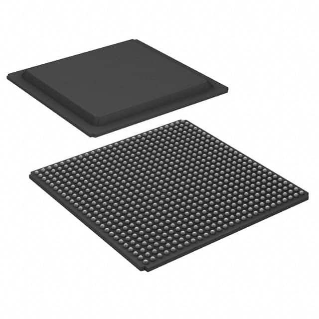
XC6SLX100-2FG676I
Overview
Product Category
The XC6SLX100-2FG676I belongs to the category of Field Programmable Gate Arrays (FPGAs).
Use
FPGAs are integrated circuits that can be programmed and reprogrammed to perform various digital functions. The XC6SLX100-2FG676I is specifically designed for high-performance applications.
Characteristics
- High-speed processing capabilities
- Configurable logic blocks
- On-chip memory
- Flexible I/O interfaces
- Low power consumption
Package
The XC6SLX100-2FG676I comes in a FG676 package, which refers to a fine-pitch ball grid array with 676 solder balls.
Essence
The essence of the XC6SLX100-2FG676I lies in its ability to provide customizable digital logic functions, allowing designers to implement complex systems on a single chip.
Packaging/Quantity
The XC6SLX100-2FG676I is typically packaged individually and is available in various quantities depending on the manufacturer's specifications.
Specifications
- Logic Cells: 101,261
- Flip-Flops: 63,360
- Block RAM: 4,860 Kb
- DSP Slices: 240
- Maximum Frequency: 550 MHz
- Operating Voltage: 1.2V
- Operating Temperature Range: -40°C to 100°C
Detailed Pin Configuration
The XC6SLX100-2FG676I has a total of 676 pins arranged in a specific configuration. For detailed pin assignments, please refer to the manufacturer's datasheet.
Functional Features
- High-speed data processing
- Reconfigurability for design flexibility
- Support for various communication protocols
- On-chip memory for efficient data storage
- Built-in digital signal processing capabilities
Advantages and Disadvantages
Advantages
- Customizable logic functions
- High-performance processing
- Flexibility in design iterations
- Reduced time-to-market for complex systems
- Lower power consumption compared to traditional ASICs
Disadvantages
- Higher cost compared to general-purpose microcontrollers
- Steeper learning curve for FPGA programming
- Limited availability of skilled FPGA designers
Working Principles
The XC6SLX100-2FG676I operates based on the principles of reconfigurable digital logic. It consists of configurable logic blocks, interconnect resources, and programmable input/output blocks. The device can be programmed using a Hardware Description Language (HDL) to define the desired functionality.
Detailed Application Field Plans
The XC6SLX100-2FG676I finds applications in various fields, including:
- Telecommunications: Used in base stations, routers, and network switches for high-speed data processing.
- Aerospace and Defense: Employed in radar systems, avionics, and military communication equipment for their performance and flexibility.
- Industrial Automation: Utilized in control systems, robotics, and machine vision applications for real-time processing and customization.
- Medical Devices: Integrated into medical imaging systems, patient monitoring devices, and diagnostic equipment for their computational power and versatility.
Detailed and Complete Alternative Models
- XC6SLX75-2FGG484C
- XC6SLX150-2FGG484C
- XC6SLX25-2FTG256C
- XC6SLX45-2FTG256C
- XC6SLX100-2CSG484C
These alternative models offer similar features and capabilities to the XC6SLX100-2FG676I, but may vary in terms of logic capacity, package type, or operating temperature range.
In conclusion, the XC6SLX100-2FG676I is a high-performance FPGA that provides customizable digital logic functions. Its flexibility, speed, and reconfigurability make it suitable for a wide range of applications in various industries.
Énumérez 10 questions et réponses courantes liées à l'application de XC6SLX100-2FG676I dans les solutions techniques
Sure! Here are 10 common questions and answers related to the application of XC6SLX100-2FG676I in technical solutions:
Q: What is XC6SLX100-2FG676I? A: XC6SLX100-2FG676I is a field-programmable gate array (FPGA) manufactured by Xilinx. It belongs to the Spartan-6 family and has 100,000 logic cells.
Q: What are the key features of XC6SLX100-2FG676I? A: Some key features include high-performance logic fabric, integrated block RAM, DSP slices, clock management resources, and support for various I/O standards.
Q: What applications can XC6SLX100-2FG676I be used for? A: XC6SLX100-2FG676I can be used in a wide range of applications such as industrial automation, telecommunications, automotive, aerospace, medical devices, and more.
Q: How can I program XC6SLX100-2FG676I? A: XC6SLX100-2FG676I can be programmed using Xilinx's Vivado Design Suite or ISE Design Suite software tools.
Q: What is the power supply requirement for XC6SLX100-2FG676I? A: The recommended power supply voltage for XC6SLX100-2FG676I is 1.2V, but it also supports other voltages depending on the specific requirements of the design.
Q: Can XC6SLX100-2FG676I interface with external devices? A: Yes, XC6SLX100-2FG676I has a variety of I/O standards and can interface with external devices such as sensors, memory, displays, communication modules, and more.
Q: What is the maximum operating frequency of XC6SLX100-2FG676I? A: The maximum operating frequency of XC6SLX100-2FG676I depends on the specific design and implementation, but it can typically reach frequencies in the range of hundreds of megahertz (MHz) to a few gigahertz (GHz).
Q: Can XC6SLX100-2FG676I be used for real-time signal processing? A: Yes, XC6SLX100-2FG676I has dedicated digital signal processing (DSP) slices that can be utilized for real-time signal processing tasks.
Q: Does XC6SLX100-2FG676I support high-speed serial communication protocols? A: Yes, XC6SLX100-2FG676I supports various high-speed serial communication protocols such as PCIe, Ethernet, USB, SATA, and more.
Q: Are there any development boards available for XC6SLX100-2FG676I? A: Yes, Xilinx offers development boards like the Spartan-6 FPGA SP601 Evaluation Kit that can be used for prototyping and testing designs based on XC6SLX100-2FG676I.
Please note that the answers provided here are general and may vary depending on the specific requirements and implementation of your technical solution.

