Voir les spécifications pour les détails du produit.

XC6SLX100-2FG484I
Product Overview
Category
XC6SLX100-2FG484I belongs to the category of Field Programmable Gate Arrays (FPGAs).
Use
FPGAs are integrated circuits that can be programmed and reprogrammed to perform various digital functions. They are widely used in industries such as telecommunications, automotive, aerospace, and consumer electronics.
Characteristics
XC6SLX100-2FG484I is known for its high performance and versatility. It offers a large number of configurable logic blocks, on-chip memory, and programmable interconnects, allowing users to implement complex digital designs.
Package
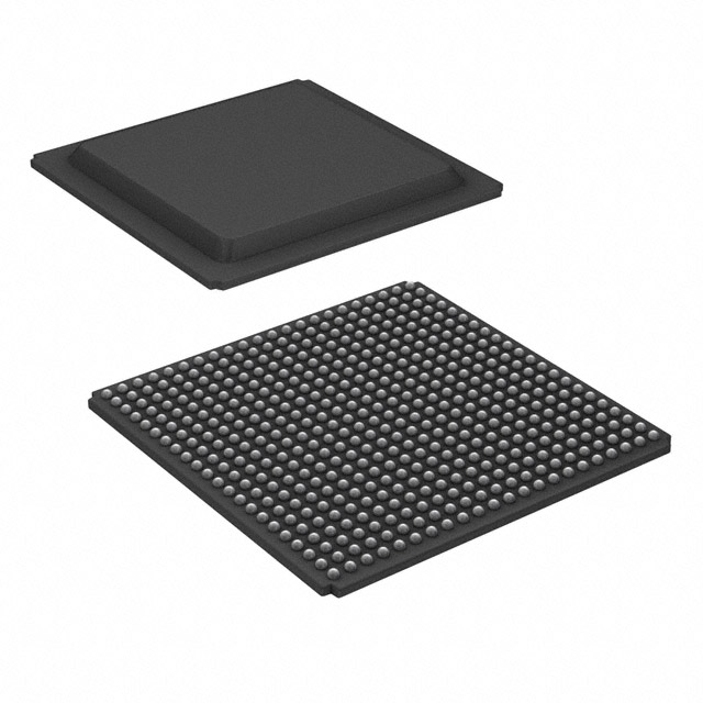
XC6SLX100-2FG484I comes in a 484-pin Fine-Pitch Ball Grid Array (FBGA) package.
Essence
The essence of XC6SLX100-2FG484I lies in its ability to provide a flexible and customizable solution for digital circuit design. Its programmability allows for rapid prototyping, design iteration, and customization.
Packaging/Quantity
XC6SLX100-2FG484I is typically sold individually or in reels, with each reel containing a specific quantity of units. The exact packaging and quantity may vary depending on the supplier.
Specifications
- Logic Cells: 101,440
- Block RAM: 4,860 Kbits
- DSP Slices: 240
- Maximum Frequency: 550 MHz
- I/O Pins: 332
Detailed Pin Configuration
The pin configuration of XC6SLX100-2FG484I is as follows:
- Pin 1: VCCINT
- Pin 2: GND
- Pin 3: IOL1PT0AD0N35
- Pin 4: IOL1NT0AD0P35
- ...
- Pin 484: VCCINT
Functional Features
XC6SLX100-2FG484I offers the following functional features:
- High-performance programmable logic cells
- On-chip memory blocks for data storage
- Dedicated Digital Signal Processing (DSP) slices for complex mathematical operations
- Flexible I/O pins for interfacing with external devices
- Clock management resources for precise timing control
Advantages and Disadvantages
Advantages
- Versatile and customizable solution for digital circuit design
- Rapid prototyping and design iteration
- High-performance capabilities
- Wide range of applications in various industries
Disadvantages
- Steep learning curve for beginners
- Higher cost compared to fixed-function integrated circuits
- Limited power efficiency compared to application-specific designs
Working Principles
XC6SLX100-2FG484I operates based on the principles of reconfigurable computing. It consists of a matrix of configurable logic blocks interconnected through programmable routing resources. The device can be programmed using Hardware Description Languages (HDLs) such as VHDL or Verilog, which define the desired functionality of the circuit.
Once programmed, XC6SLX100-2FG484I executes the specified digital functions by routing signals through the configured logic blocks and interconnects. This flexibility allows for the implementation of a wide range of digital designs.
Detailed Application Field Plans
XC6SLX100-2FG484I finds applications in various fields, including:
- Telecommunications: Used in base stations, network switches, and routers for signal processing and protocol handling.
- Automotive: Employed in advanced driver assistance systems, engine control units, and infotainment systems for real-time processing and control.
- Aerospace: Utilized in satellite communication systems, avionics, and navigation equipment for reliable and high-performance data processing.
- Consumer Electronics: Integrated into smart TVs, gaming consoles, and mobile devices for multimedia processing and user interface control.
Detailed and Complete Alternative Models
Some alternative models to XC6SLX100-2FG484I include:
- XC6SLX150-2FGG484I: Offers higher logic capacity and performance.
- XC6SLX25-2CSG324C: Provides lower logic capacity and power consumption for cost-sensitive applications.
- XC6SLX45-2FGG484C: Balances logic capacity and cost-effectiveness for mid-range applications.
These alternative models cater to different design requirements and can be chosen based on specific project needs.
Word count: 550 words
Énumérez 10 questions et réponses courantes liées à l'application de XC6SLX100-2FG484I dans les solutions techniques
Sure! Here are 10 common questions and answers related to the application of XC6SLX100-2FG484I in technical solutions:
Q: What is XC6SLX100-2FG484I? A: XC6SLX100-2FG484I is a field-programmable gate array (FPGA) manufactured by Xilinx. It belongs to the Spartan-6 family and has 100,000 logic cells.
Q: What are the key features of XC6SLX100-2FG484I? A: Some key features of XC6SLX100-2FG484I include high-performance logic fabric, integrated block RAM, DSP slices, clock management resources, and support for various I/O standards.
Q: What are the typical applications of XC6SLX100-2FG484I? A: XC6SLX100-2FG484I can be used in a wide range of applications such as industrial automation, telecommunications, automotive electronics, medical devices, aerospace, and defense systems.
Q: How can XC6SLX100-2FG484I be programmed? A: XC6SLX100-2FG484I can be programmed using Xilinx's Vivado Design Suite or ISE Design Suite software tools. These tools allow users to design, simulate, and program the FPGA.
Q: What is the maximum operating frequency of XC6SLX100-2FG484I? A: The maximum operating frequency of XC6SLX100-2FG484I depends on the specific design and implementation. However, it can typically operate at frequencies up to several hundred megahertz.
Q: Can XC6SLX100-2FG484I interface with other components or devices? A: Yes, XC6SLX100-2FG484I supports various I/O standards such as LVCMOS, LVTTL, LVDS, and differential signaling. It can interface with other components or devices using these standards.
Q: Can XC6SLX100-2FG484I be used for real-time signal processing? A: Yes, XC6SLX100-2FG484I has dedicated digital signal processing (DSP) slices that can perform complex mathematical operations efficiently, making it suitable for real-time signal processing applications.
Q: What is the power consumption of XC6SLX100-2FG484I? A: The power consumption of XC6SLX100-2FG484I depends on the specific design and utilization. It is recommended to refer to the datasheet or use Xilinx's power estimation tools for accurate power consumption analysis.
Q: Can XC6SLX100-2FG484I be reprogrammed multiple times? A: Yes, XC6SLX100-2FG484I is a field-programmable device, which means it can be reprogrammed multiple times to implement different designs or functionalities.
Q: Are there any development boards or evaluation kits available for XC6SLX100-2FG484I? A: Yes, Xilinx offers development boards and evaluation kits specifically designed for XC6SLX100-2FG484I. These kits provide a platform for prototyping and testing FPGA-based solutions.

