Voir les spécifications pour les détails du produit.

XC6SLX100-2CSG484C
Product Overview
Category
The XC6SLX100-2CSG484C belongs to the category of Field Programmable Gate Arrays (FPGAs).
Use
FPGAs are integrated circuits that can be programmed after manufacturing. The XC6SLX100-2CSG484C is specifically designed for high-performance applications, such as digital signal processing, telecommunications, and embedded systems.
Characteristics
- High-performance FPGA with advanced features
- Low power consumption
- Large number of logic cells and I/O pins
- Flexible and reconfigurable design
Package
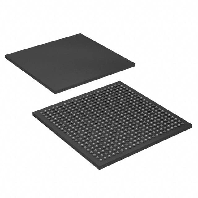
The XC6SLX100-2CSG484C comes in a 484-pin Ceramic Quad Flat Pack (CQFP) package.
Essence
The essence of the XC6SLX100-2CSG484C lies in its ability to provide a customizable hardware platform for various applications, allowing designers to implement complex digital systems efficiently.
Packaging/Quantity
The XC6SLX100-2CSG484C is typically sold individually or in reels, with each reel containing a specific quantity of units. The exact packaging and quantity may vary depending on the supplier.
Specifications
- Logic Cells: 101,261
- Flip-Flops: 63,280
- Block RAM: 4,860 Kbits
- DSP Slices: 240
- Maximum Frequency: 550 MHz
- Operating Voltage: 1.2V
- Operating Temperature Range: -40°C to +100°C
Detailed Pin Configuration
The XC6SLX100-2CSG484C has a total of 484 pins, each serving a specific purpose. The pin configuration includes dedicated input/output pins, clock pins, power supply pins, and configuration pins. For a detailed pinout diagram and description, please refer to the manufacturer's datasheet.
Functional Features
- High-speed serial connectivity
- Integrated memory blocks for efficient data storage
- Flexible clock management resources
- Built-in digital signal processing capabilities
- Support for various communication protocols
- On-chip configuration memory for easy reprogramming
Advantages and Disadvantages
Advantages
- Versatile and customizable hardware platform
- High-performance capabilities
- Low power consumption
- Reconfigurable design allows for iterative development
- Wide range of available tools and support from the manufacturer and community
Disadvantages
- Steep learning curve for beginners
- Higher cost compared to other programmable logic devices
- Limited availability of alternative models with similar specifications
Working Principles
The XC6SLX100-2CSG484C operates based on the principles of configurable logic. It consists of a large number of configurable logic blocks (CLBs) interconnected through programmable routing resources. The device can be programmed using Hardware Description Languages (HDLs) such as VHDL or Verilog, which define the desired functionality of the circuit. Once programmed, the FPGA executes the specified logic operations.
Detailed Application Field Plans
The XC6SLX100-2CSG484C finds applications in various fields, including:
- Digital Signal Processing: The FPGA's high-performance capabilities make it suitable for implementing complex algorithms used in audio and video processing, image recognition, and communications systems.
- Telecommunications: FPGAs are widely used in telecommunications infrastructure for tasks like protocol conversion, encryption/decryption, and network packet processing.
- Embedded Systems: The XC6SLX100-2CSG484C can be utilized in embedded systems for controlling and interfacing with external devices, providing flexibility and real-time processing capabilities.
Detailed and Complete Alternative Models
While the XC6SLX100-2CSG484C offers a unique combination of features, there are alternative FPGA models available in the market with similar capabilities. Some notable alternatives include:
- Xilinx XC7A100T-2CSG324C
- Intel (formerly Altera) EP4CE115F29C7N
- Lattice Semiconductor LFXP6C-4TN144C
These alternative models provide comparable performance and functionality, allowing designers to choose the most suitable option for their specific requirements.
In conclusion, the XC6SLX100-2CSG484C is a high-performance FPGA that offers flexibility, reconfigurability, and advanced features. Its applications span across digital signal processing, telecommunications, and embedded systems. While it has advantages such as versatility and low power consumption, it also has disadvantages like a steep learning curve and higher cost. Understanding its working principles and considering alternative models can help designers make informed decisions when selecting an FPGA for their projects.
Énumérez 10 questions et réponses courantes liées à l'application de XC6SLX100-2CSG484C dans les solutions techniques
Sure! Here are 10 common questions and answers related to the application of XC6SLX100-2CSG484C in technical solutions:
Question: What is the XC6SLX100-2CSG484C?
Answer: The XC6SLX100-2CSG484C is a field-programmable gate array (FPGA) from Xilinx, which offers programmable logic and digital signal processing capabilities.Question: What are the key features of the XC6SLX100-2CSG484C?
Answer: The key features include 100,000 logic cells, 352 I/O pins, 36 DSP slices, 4.9 Mb of block RAM, and support for various communication protocols.Question: What are some typical applications of the XC6SLX100-2CSG484C?
Answer: It is commonly used in applications such as industrial automation, telecommunications, video processing, medical devices, and aerospace systems.Question: How can I program the XC6SLX100-2CSG484C?
Answer: The XC6SLX100-2CSG484C can be programmed using Xilinx's Vivado Design Suite or ISE Design Suite software tools.Question: What is the power supply requirement for the XC6SLX100-2CSG484C?
Answer: The XC6SLX100-2CSG484C typically operates at a voltage range of 1.14V to 1.26V, with a maximum power consumption of around 3W.Question: Can I interface the XC6SLX100-2CSG484C with other components or devices?
Answer: Yes, the XC6SLX100-2CSG484C supports various communication protocols such as UART, SPI, I2C, Ethernet, and PCIe, allowing easy interfacing with other components or devices.Question: What is the maximum clock frequency supported by the XC6SLX100-2CSG484C?
Answer: The maximum clock frequency depends on the design and implementation, but it can typically reach up to 500 MHz.Question: Can I use the XC6SLX100-2CSG484C for real-time signal processing?
Answer: Yes, the XC6SLX100-2CSG484C's DSP slices and high-speed I/O capabilities make it suitable for real-time signal processing applications.Question: Does the XC6SLX100-2CSG484C support secure boot or encryption features?
Answer: Yes, the XC6SLX100-2CSG484C supports bitstream encryption and authentication features to ensure secure boot and protection of intellectual property.Question: Are there any development boards available for prototyping with the XC6SLX100-2CSG484C?
Answer: Yes, Xilinx offers various development boards like the Spartan-6 FPGA SP601 Evaluation Kit, which can be used for prototyping and testing with the XC6SLX100-2CSG484C.
Please note that these answers are general and may vary depending on specific requirements and configurations.

