

Voir les spécifications pour les détails du produit.
XC5VLX330-2FFG1760C
Product Overview
Category
The XC5VLX330-2FFG1760C belongs to the category of Field Programmable Gate Arrays (FPGAs).
Use
FPGAs are integrated circuits that can be programmed and reprogrammed to perform various digital functions. The XC5VLX330-2FFG1760C is specifically designed for high-performance applications that require complex logic functions.
Characteristics
- High-performance FPGA with advanced features
- Large capacity and high-speed processing capabilities
- Flexible and reconfigurable design
- Suitable for demanding applications in industries such as telecommunications, aerospace, and automotive
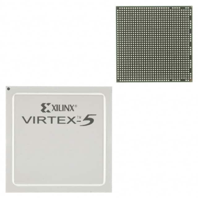
Package
The XC5VLX330-2FFG1760C comes in a Fine-Pitch Ball Grid Array (FBGA) package.
Essence
The essence of the XC5VLX330-2FFG1760C lies in its ability to provide a customizable and high-performance solution for complex digital logic requirements.
Packaging/Quantity
The XC5VLX330-2FFG1760C is typically packaged individually and is available in various quantities depending on the customer's requirements.
Specifications
- Logic Cells: 330,000
- Block RAM: 4,608 Kbits
- DSP Slices: 864
- Maximum I/Os: 1,760
- Operating Voltage: 1.2V
- Operating Temperature Range: -40°C to +100°C
- Package Type: FBGA
- Package Pins: 1760
- Speed Grade: -2
Detailed Pin Configuration
The XC5VLX330-2FFG1760C has a total of 1760 pins, each serving a specific purpose in the FPGA's functionality. A detailed pin configuration diagram can be found in the product datasheet.
Functional Features
- High-speed processing capabilities
- Configurable logic blocks for custom designs
- Built-in DSP slices for efficient signal processing
- Flexible I/O options for interfacing with external devices
- On-chip memory resources for data storage and retrieval
Advantages and Disadvantages
Advantages
- High-performance and customizable solution
- Reconfigurable design allows for flexibility in adapting to changing requirements
- Suitable for demanding applications that require complex logic functions
- Large capacity and high-speed processing capabilities
Disadvantages
- Higher cost compared to other programmable logic devices
- Steeper learning curve for programming and utilizing the FPGA's full potential
- Requires specialized tools and expertise for development and debugging
Working Principles
The XC5VLX330-2FFG1760C operates based on the principles of digital logic. It consists of configurable logic blocks, interconnects, and various resources such as memory and DSP slices. The FPGA can be programmed using Hardware Description Languages (HDL) like VHDL or Verilog to define the desired functionality. Once programmed, the FPGA executes the logic functions by routing signals through the configurable interconnects and logic blocks.
Detailed Application Field Plans
The XC5VLX330-2FFG1760C finds applications in various industries where high-performance and customizable digital logic solutions are required. Some specific application fields include:
- Telecommunications: Used in base stations, routers, and network switches for high-speed data processing and protocol handling.
- Aerospace: Employed in avionics systems for tasks such as radar signal processing, flight control, and communication interfaces.
- Automotive: Utilized in advanced driver assistance systems (ADAS), engine control units (ECUs), and infotainment systems for real-time processing and control.
Detailed and Complete Alternative Models
- XC7A200T-2FBG676C: A high-performance FPGA with similar capabilities but a different package and pin configuration.
- XC6SLX150-3FGG484C: A lower-cost FPGA with slightly reduced capacity and speed, suitable for less demanding applications.
- XC7K325T-2FFG900C: An advanced FPGA with enhanced features and higher logic capacity, ideal for complex designs.
These alternative models provide options based on specific requirements and constraints, allowing users to choose the most suitable FPGA for their application needs.
Word count: 560 words
Énumérez 10 questions et réponses courantes liées à l'application de XC5VLX330-2FFG1760C dans les solutions techniques
Sure! Here are 10 common questions and answers related to the application of XC5VLX330-2FFG1760C in technical solutions:
Question: What is XC5VLX330-2FFG1760C?
Answer: XC5VLX330-2FFG1760C is a field-programmable gate array (FPGA) from Xilinx, which offers high-performance processing capabilities for various technical applications.Question: What are the key features of XC5VLX330-2FFG1760C?
Answer: Some key features of XC5VLX330-2FFG1760C include a large number of logic cells, high-speed serial transceivers, embedded memory blocks, and advanced DSP capabilities.Question: In what technical solutions can XC5VLX330-2FFG1760C be used?
Answer: XC5VLX330-2FFG1760C can be used in a wide range of technical solutions, including telecommunications, aerospace, defense, industrial automation, and scientific research.Question: What is the maximum operating frequency of XC5VLX330-2FFG1760C?
Answer: The maximum operating frequency of XC5VLX330-2FFG1760C is typically around 550 MHz, but it can vary depending on the specific design and implementation.Question: How much logic capacity does XC5VLX330-2FFG1760C offer?
Answer: XC5VLX330-2FFG1760C has a logic capacity of approximately 330,000 logic cells, which allows for complex and highly integrated designs.Question: Can XC5VLX330-2FFG1760C support high-speed serial communication?
Answer: Yes, XC5VLX330-2FFG1760C is equipped with high-speed serial transceivers that support various protocols like PCIe, SATA, and Ethernet.Question: Does XC5VLX330-2FFG1760C have built-in memory?
Answer: Yes, XC5VLX330-2FFG1760C has embedded memory blocks (BRAM) that can be used for storing data or implementing lookup tables.Question: What are the power requirements for XC5VLX330-2FFG1760C?
Answer: The power requirements for XC5VLX330-2FFG1760C typically include a core voltage of 1.0V and auxiliary voltages for I/O banks.Question: Can XC5VLX330-2FFG1760C be reprogrammed after deployment?
Answer: Yes, XC5VLX330-2FFG1760C is a field-programmable device, which means it can be reprogrammed even after it has been deployed in a technical solution.Question: Are there any development tools available for programming XC5VLX330-2FFG1760C?
Answer: Yes, Xilinx provides a range of development tools, such as Vivado Design Suite, which allows designers to program and configure XC5VLX330-2FFG1760C efficiently.
Please note that the answers provided here are general and may vary depending on specific requirements and implementations.