

Voir les spécifications pour les détails du produit.
XC3S700A-4FG400I
Product Overview
Category
The XC3S700A-4FG400I belongs to the category of Field-Programmable Gate Arrays (FPGAs).
Use
FPGAs are integrated circuits that can be programmed and reprogrammed to perform various digital functions. The XC3S700A-4FG400I is specifically designed for high-performance applications that require complex logic functions.
Characteristics
- High-density FPGA with 700,000 system gates
- Advanced programmable logic architecture
- Low power consumption
- Fast performance with high-speed interfaces
- Flexible and customizable design options
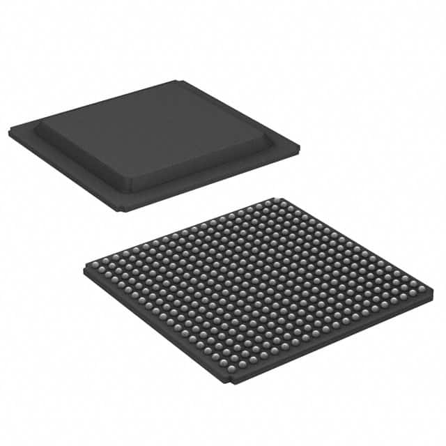
Package
The XC3S700A-4FG400I comes in a FG400 package, which refers to a fine-pitch ball grid array (BGA) package with 400 balls. This package provides excellent thermal and electrical performance.
Essence
The essence of the XC3S700A-4FG400I lies in its ability to provide a highly configurable and flexible platform for implementing complex digital designs. It allows designers to create custom logic circuits without the need for traditional fixed-function integrated circuits.
Packaging/Quantity
The XC3S700A-4FG400I is typically packaged individually and is available in various quantities depending on the manufacturer or distributor.
Specifications
- System Gates: 700,000
- Logic Cells: 68,200
- Block RAM: 2,592 Kbits
- DSP Slices: 740
- Maximum Frequency: 550 MHz
- I/O Pins: 356
Detailed Pin Configuration
The XC3S700A-4FG400I has a total of 400 pins arranged in a fine-pitch ball grid array (BGA) package. Each pin serves a specific purpose, including input, output, power supply, and configuration. A detailed pin configuration diagram can be found in the product datasheet.
Functional Features
- High-performance programmable logic with advanced architecture
- Configurable I/O standards and voltage levels
- On-chip memory blocks for efficient data storage
- Dedicated digital signal processing (DSP) slices for complex mathematical operations
- Built-in clock management resources for precise timing control
- Support for various communication protocols and interfaces
Advantages and Disadvantages
Advantages
- Flexibility: FPGAs offer the ability to reconfigure the hardware, allowing for rapid prototyping and design iterations.
- Customizability: The XC3S700A-4FG400I allows designers to create tailored solutions for specific applications.
- High Performance: With its large number of logic cells and high-speed interfaces, this FPGA can handle complex tasks efficiently.
Disadvantages
- Complexity: Designing for FPGAs requires specialized knowledge and expertise.
- Power Consumption: FPGAs tend to consume more power compared to fixed-function integrated circuits.
- Cost: FPGAs can be more expensive than traditional integrated circuits, especially for low-volume production.
Working Principles
The XC3S700A-4FG400I operates based on the principles of reconfigurable computing. It consists of an array of configurable logic blocks interconnected through programmable routing resources. These logic blocks can be programmed to implement desired digital functions by configuring the interconnections and functionality of each block.
Detailed Application Field Plans
The XC3S700A-4FG400I finds applications in various fields, including:
- Telecommunications: Used in base stations, routers, and network switches for high-speed data processing and protocol handling.
- Aerospace and Defense: Employed in radar systems, avionics, and military communication equipment for their high performance and flexibility.
- Industrial Automation: Utilized in control systems, robotics, and machine vision applications for real-time data processing and control.
- Medical Devices: Integrated into medical imaging systems, patient monitoring devices, and laboratory equipment to handle complex algorithms and signal processing.
Detailed and Complete Alternative Models
- XC7A100T-2FGG484I: A newer FPGA model with enhanced performance and higher logic capacity.
- XC6SLX150-3FGG484C: An alternative FPGA with lower power consumption and a smaller form factor.
- XC2S200E-6FGG456C: A cost-effective FPGA option suitable for simpler designs with moderate logic requirements.
These alternative models provide different trade-offs in terms of performance, power consumption, and cost, allowing designers to choose the most suitable FPGA for their specific application needs.
In conclusion, the XC3S700A-4FG400I is a high-density FPGA that offers flexibility, customizability, and high performance for various digital design applications. Its advanced architecture, extensive I/O capabilities, and configurable resources make it a versatile choice for demanding projects in telecommunications, aerospace, industrial automation, and medical fields. Designers can also consider alternative models
Énumérez 10 questions et réponses courantes liées à l'application de XC3S700A-4FG400I dans les solutions techniques
Sure! Here are 10 common questions and answers related to the application of XC3S700A-4FG400I in technical solutions:
Q: What is XC3S700A-4FG400I? A: XC3S700A-4FG400I is a field-programmable gate array (FPGA) manufactured by Xilinx. It is designed for high-performance applications and offers a large number of logic cells, I/O pins, and other features.
Q: What are the key features of XC3S700A-4FG400I? A: Some key features include 700K system gates, 36K logic cells, 900MHz internal clock frequency, 400 I/O pins, and support for various communication protocols.
Q: What are the typical applications of XC3S700A-4FG400I? A: XC3S700A-4FG400I is commonly used in applications such as digital signal processing, video and image processing, telecommunications, industrial control systems, and high-speed data acquisition.
Q: How can I program XC3S700A-4FG400I? A: XC3S700A-4FG400I can be programmed using Xilinx's Vivado Design Suite or ISE Design Suite software. These tools allow you to write your design in a hardware description language (HDL) like VHDL or Verilog and then generate a bitstream file to program the FPGA.
Q: Can XC3S700A-4FG400I be reprogrammed after it has been programmed once? A: Yes, XC3S700A-4FG400I is a reprogrammable FPGA. You can erase the existing configuration and program it with a new design as many times as needed.
Q: What voltage levels does XC3S700A-4FG400I support? A: XC3S700A-4FG400I supports both 3.3V and 1.8V voltage levels for I/O pins, allowing compatibility with a wide range of external devices.
Q: Can XC3S700A-4FG400I interface with other components or devices? A: Yes, XC3S700A-4FG400I has various I/O standards and can interface with different components such as memories, sensors, displays, communication modules, and more.
Q: Does XC3S700A-4FG400I have any built-in peripherals? A: No, XC3S700A-4FG400I is a pure FPGA without any built-in peripherals. However, you can implement custom peripherals using the available logic cells and I/O pins.
Q: What are the power requirements for XC3S700A-4FG400I? A: The typical operating voltage for XC3S700A-4FG400I is 1.2V, but it also requires additional voltages for I/O banks and configuration. Please refer to the datasheet for detailed power supply recommendations.
Q: Are there any development boards or evaluation kits available for XC3S700A-4FG400I? A: Yes, Xilinx provides development boards and evaluation kits that include XC3S700A-4FG400I, allowing you to quickly prototype and test your designs. These boards often come with documentation and example projects to help you get started.
Please note that these answers are general and may vary depending on specific requirements and use cases. It's always recommended to refer to the official documentation and datasheets for accurate and up-to-date information.