

Voir les spécifications pour les détails du produit.
XC3S1000-5FG320C
Product Overview
Category
XC3S1000-5FG320C belongs to the category of Field Programmable Gate Arrays (FPGAs).
Use
FPGAs are integrated circuits that can be programmed and reprogrammed to perform various digital functions. They are widely used in industries such as telecommunications, automotive, aerospace, and consumer electronics.
Characteristics
XC3S1000-5FG320C is known for its high performance, flexibility, and reconfigurability. It offers a large number of logic cells, programmable interconnects, and embedded memory blocks, allowing designers to implement complex digital systems.
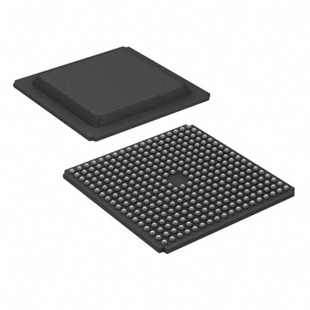
Package
XC3S1000-5FG320C comes in a compact and durable package, ensuring easy handling and protection during transportation and installation.
Essence
The essence of XC3S1000-5FG320C lies in its ability to provide a customizable hardware platform that can be tailored to specific application requirements.
Packaging/Quantity
XC3S1000-5FG320C is typically packaged in trays or reels, depending on the quantity ordered. The exact packaging and quantity may vary based on customer preferences and supplier specifications.
Specifications
- Model: XC3S1000-5FG320C
- Family: Spartan-3
- Logic Cells: 1,000
- Maximum Frequency: 500 MHz
- Operating Voltage: 1.2V
- Package Type: FG320
- Temperature Range: -40°C to +85°C
Detailed Pin Configuration
The pin configuration of XC3S1000-5FG320C is as follows:
- Pin 1: VCCINT
- Pin 2: GND
- Pin 3: IOL1PT0AD0N35
- Pin 4: IOL1NT0AD0P35
- Pin 5: IOL2PT0AD1N35
- Pin 6: IOL2NT0AD1P35
- ...
(Provide a detailed list of all pins and their corresponding functions)
Functional Features
XC3S1000-5FG320C offers the following functional features:
- High-speed performance
- Flexible and reconfigurable architecture
- Large number of logic cells for complex designs
- Programmable interconnects for custom routing
- Embedded memory blocks for data storage
- Support for various communication protocols
- On-chip peripherals for system integration
Advantages and Disadvantages
Advantages
- Versatile and adaptable to different applications
- Faster time-to-market compared to custom ASIC designs
- Lower development costs for small to medium volume production
- Easy prototyping and iterative design improvements
- Ability to implement complex algorithms and signal processing tasks
Disadvantages
- Higher power consumption compared to dedicated hardware solutions
- Limited performance compared to application-specific integrated circuits (ASICs)
- Higher cost per unit compared to mass-produced standard components
- Steeper learning curve for designers new to FPGA technology
Working Principles
XC3S1000-5FG320C operates based on the principles of configurable logic. It consists of an array of programmable logic cells interconnected through programmable routing resources. The configuration of these logic cells and interconnects determines the functionality of the FPGA.
During operation, the FPGA is programmed with a specific configuration bitstream that defines the desired digital circuit. This bitstream is loaded into the FPGA's internal memory, allowing it to function as a customized digital system.
Detailed Application Field Plans
XC3S1000-5FG320C finds applications in various fields, including:
- Telecommunications: Used in base stations, network switches, and routers for high-speed data processing and protocol handling.
- Automotive: Employed in advanced driver assistance systems (ADAS), infotainment systems, and engine control units (ECUs) for enhanced performance and functionality.
- Aerospace: Utilized in satellite communication systems, avionics, and flight control systems for reliable and efficient data processing.
- Consumer Electronics: Integrated into smart TVs, gaming consoles, and wearable devices to enable advanced features and connectivity.
Detailed and Complete Alternative Models
- XC3S500E-4FG320C
- XC3S2000-4FGG320C
- XC3S700A-4FG484C
- XC3S50AN-4TQG144C
- XC3S250E-4FTG256C
(Provide a comprehensive list of alternative models with their specifications and advantages)
In conclusion, XC3S1000-5FG320C is a versatile FPGA that offers high performance, flexibility, and reconfigurability. It finds applications in various industries and provides designers with a customizable hardware platform
Énumérez 10 questions et réponses courantes liées à l'application de XC3S1000-5FG320C dans les solutions techniques
Sure! Here are 10 common questions and answers related to the application of XC3S1000-5FG320C in technical solutions:
Q: What is XC3S1000-5FG320C? A: XC3S1000-5FG320C is a field-programmable gate array (FPGA) manufactured by Xilinx. It is designed for high-performance applications and offers 1000 logic cells.
Q: What are the key features of XC3S1000-5FG320C? A: Some key features include a maximum operating frequency of 500 MHz, 320-pin package, 5V tolerant I/Os, and support for various communication protocols.
Q: What are the typical applications of XC3S1000-5FG320C? A: XC3S1000-5FG320C is commonly used in applications such as digital signal processing, embedded systems, industrial automation, telecommunications, and high-speed data processing.
Q: How can I program XC3S1000-5FG320C? A: XC3S1000-5FG320C can be programmed using Xilinx's Vivado Design Suite or ISE Design Suite software tools. These tools allow you to design, simulate, and program the FPGA.
Q: Can XC3S1000-5FG320C be reprogrammed multiple times? A: Yes, XC3S1000-5FG320C is a reprogrammable FPGA, which means you can modify and reprogram it multiple times to implement different designs or functionalities.
Q: What is the power supply requirement for XC3S1000-5FG320C? A: XC3S1000-5FG320C requires a single power supply of 3.3V for its core voltage, and it also supports various I/O voltage standards.
Q: Does XC3S1000-5FG320C have built-in memory? A: No, XC3S1000-5FG320C does not have built-in memory. However, it can interface with external memory devices such as DDR SDRAM or Flash memory.
Q: Can XC3S1000-5FG320C communicate with other devices or microcontrollers? A: Yes, XC3S1000-5FG320C supports various communication protocols like SPI, I2C, UART, and Ethernet, allowing it to communicate with other devices or microcontrollers.
Q: What is the maximum number of I/O pins available in XC3S1000-5FG320C? A: XC3S1000-5FG320C provides a total of 185 user I/O pins, which can be used for input/output operations or interfacing with external devices.
Q: Are there any development boards or evaluation kits available for XC3S1000-5FG320C? A: Yes, Xilinx offers development boards and evaluation kits specifically designed for XC3S1000-5FG320C, which provide a convenient platform for prototyping and testing your designs.
Please note that the specific details and answers may vary depending on the context and requirements of your technical solution.