

Voir les spécifications pour les détails du produit.
XC3S1000-4FG320I
Product Overview
Category
XC3S1000-4FG320I belongs to the category of Field Programmable Gate Arrays (FPGAs).
Use
FPGAs are integrated circuits that can be programmed and reprogrammed to perform various digital functions. They are widely used in industries such as telecommunications, automotive, aerospace, and consumer electronics.
Characteristics
- High flexibility: FPGAs can be customized to perform specific tasks by programming the logic gates and interconnections.
- Parallel processing: FPGAs can execute multiple operations simultaneously, making them suitable for applications requiring high-speed data processing.
- Reconfigurability: FPGAs can be reprogrammed multiple times, allowing for easy updates and modifications.
- Low power consumption: Compared to traditional application-specific integrated circuits (ASICs), FPGAs consume less power.
Package
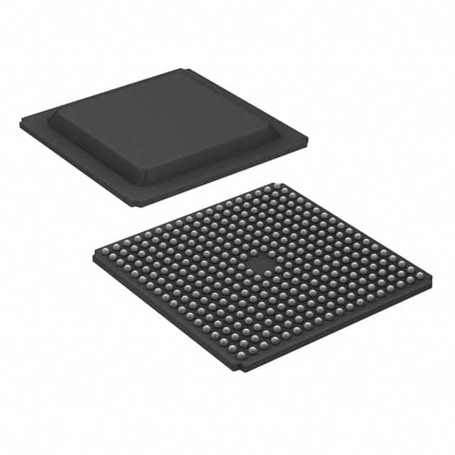
XC3S1000-4FG320I is available in a 320-pin Fine-Pitch Ball Grid Array (FBGA) package.
Essence
The essence of XC3S1000-4FG320I lies in its ability to provide a flexible and customizable solution for digital circuit design and implementation.
Packaging/Quantity
XC3S1000-4FG320I is typically packaged individually and is available in various quantities depending on the manufacturer and distributor.
Specifications
- FPGA Family: Spartan-3
- Logic Cells: 1,016
- Number of I/Os: 317
- Operating Voltage: 1.2V
- Maximum Frequency: 400 MHz
- Embedded Memory: 576 Kb
- Configuration Memory: 4 Mb
- Package Type: FBGA
- Temperature Range: -40°C to +100°C
Detailed Pin Configuration
The XC3S1000-4FG320I FPGA has a total of 320 pins, each serving a specific purpose in the circuit design. The pin configuration includes input/output (I/O) pins, power supply pins, ground pins, and configuration pins. A detailed pinout diagram can be found in the product datasheet.
Functional Features
XC3S1000-4FG320I offers several functional features that make it suitable for a wide range of applications:
- High-speed data processing: With a maximum operating frequency of 400 MHz, this FPGA can handle complex computations and real-time data processing tasks efficiently.
- Flexible I/O capabilities: The 317 I/O pins allow for seamless integration with external devices and peripherals.
- Embedded memory: The 576 Kb of embedded memory provides additional storage for data buffering and temporary storage requirements.
- Reconfigurability: The ability to reprogram the FPGA enables quick updates and modifications without the need for hardware changes.
- Low power consumption: The XC3S1000-4FG320I is designed to minimize power consumption, making it suitable for battery-powered applications.
Advantages and Disadvantages
Advantages
- Flexibility and customization options
- Parallel processing capabilities
- Reconfigurability for easy updates
- Lower power consumption compared to ASICs
Disadvantages
- Higher cost compared to fixed-function integrated circuits
- Steeper learning curve for programming and design
Working Principles
FPGAs like XC3S1000-4FG320I consist of an array of configurable logic blocks (CLBs) interconnected by programmable interconnects. These CLBs contain look-up tables (LUTs), flip-flops, and other components that can be programmed to implement desired digital functions. The interconnects allow for routing signals between different CLBs, enabling complex circuit designs.
The working principle involves configuring the FPGA using a Hardware Description Language (HDL) such as VHDL or Verilog. The HDL code describes the desired circuit functionality, which is then synthesized and implemented on the FPGA using specialized software tools.
Detailed Application Field Plans
XC3S1000-4FG320I finds applications in various fields, including:
- Telecommunications: Used for signal processing, protocol conversion, and network optimization.
- Automotive: Employed in advanced driver-assistance systems (ADAS), engine control units (ECUs), and infotainment systems.
- Aerospace: Utilized in avionics, radar systems, and satellite communication.
- Consumer Electronics: Found in high-definition televisions, gaming consoles, and audio/video processing devices.
Detailed and Complete Alternative Models
Some alternative models to XC3S1000-4FG320I that offer similar functionalities include:
- XC3S500E-4FG320C
- XC3S200-4FTG256C
- XC3S700A-4FG484I
- XC3S400-4PQ208C
These models vary in terms of logic capacity, I/O count,
Énumérez 10 questions et réponses courantes liées à l'application de XC3S1000-4FG320I dans les solutions techniques
Sure! Here are 10 common questions and answers related to the application of XC3S1000-4FG320I in technical solutions:
Q: What is XC3S1000-4FG320I? A: XC3S1000-4FG320I is a field-programmable gate array (FPGA) manufactured by Xilinx. It is designed for high-performance applications and offers 1000 logic cells.
Q: What are the key features of XC3S1000-4FG320I? A: Some key features include 1000 logic cells, 32,640 flip-flops, 64 DSP slices, 16 multipliers, and support for various I/O standards.
Q: What are the typical applications of XC3S1000-4FG320I? A: XC3S1000-4FG320I can be used in a wide range of applications such as digital signal processing, communication systems, industrial automation, and embedded systems.
Q: How can I program XC3S1000-4FG320I? A: XC3S1000-4FG320I can be programmed using Xilinx's Vivado Design Suite or ISE Design Suite software tools. These tools allow you to design and implement your FPGA-based solution.
Q: What is the maximum clock frequency supported by XC3S1000-4FG320I? A: The maximum clock frequency supported by XC3S1000-4FG320I depends on the specific design and implementation. However, it can typically operate at frequencies up to several hundred megahertz.
Q: Can XC3S1000-4FG320I interface with other components or devices? A: Yes, XC3S1000-4FG320I supports various I/O standards such as LVCMOS, LVTTL, and LVDS, allowing it to interface with a wide range of components and devices.
Q: What is the power supply requirement for XC3S1000-4FG320I? A: XC3S1000-4FG320I requires a single 1.2V core voltage supply and a separate 3.3V auxiliary supply for configuration and I/O banks.
Q: Can XC3S1000-4FG320I be reprogrammed after deployment? A: Yes, XC3S1000-4FG320I is a field-programmable device, which means it can be reprogrammed even after it has been deployed in a system.
Q: Are there any development boards available for XC3S1000-4FG320I? A: Yes, Xilinx offers development boards like the Spartan-3E Starter Kit that include XC3S1000-4FG320I, allowing you to prototype and test your designs.
Q: Where can I find more information about XC3S1000-4FG320I? A: You can find more detailed information about XC3S1000-4FG320I in the datasheet provided by Xilinx. Additionally, Xilinx's website and online forums are great resources for technical documentation and community support.
Please note that the specific details and answers may vary depending on the context and requirements of your technical solution.