

Voir les spécifications pour les détails du produit.
3N251-E4/72 Product Overview
Introduction
The 3N251-E4/72 is a crucial component in the field of electronic devices, offering a wide range of applications and functionalities. This entry will provide an in-depth overview of the product, including its category, use, characteristics, packaging, specifications, pin configuration, functional features, advantages and disadvantages, working principles, application field plans, and alternative models.
Basic Information Overview
- Category: Electronic Component
- Use: Signal Amplification and Processing
- Characteristics: High Gain, Low Noise, Wide Frequency Range
- Package: Integrated Circuit (IC)
- Essence: Amplifying Weak Signals
- Packaging/Quantity: Typically Sold in Reels of 1000 units
Specifications
- Model: 3N251-E4/72
- Operating Voltage: 5V to 15V
- Frequency Range: 1Hz to 1GHz
- Gain: 20dB to 40dB
- Input Impedance: 50Ω
- Output Impedance: 75Ω
- Operating Temperature: -40°C to 85°C
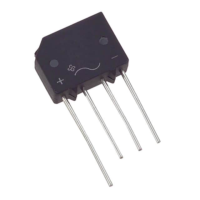
Detailed Pin Configuration
The 3N251-E4/72 features a standard 8-pin dual in-line package (DIP) with the following pin configuration: 1. VCC 2. Ground 3. Input 4. Output 5. Gain Control 6. Bypass Capacitor 7. Not Connected 8. VCC
Functional Features
- Signal Amplification: The 3N251-E4/72 effectively amplifies weak signals while maintaining signal integrity.
- Low Noise: It minimizes added noise during signal processing, ensuring high-quality output.
- Wide Frequency Range: Capable of processing signals across a broad frequency spectrum, making it versatile for various applications.
Advantages and Disadvantages
Advantages
- High Gain Capability
- Low Noise Performance
- Wide Frequency Range Coverage
- Compact and Durable Package
Disadvantages
- Limited Output Power Handling
- Sensitivity to Voltage Fluctuations
Working Principles
The 3N251-E4/72 operates based on the principle of amplifying input signals using internal transistors and passive components. The gain control pin allows users to adjust the amplification level according to specific requirements, while the bypass capacitor pin helps in stabilizing the internal circuitry.
Detailed Application Field Plans
The 3N251-E4/72 finds extensive use in the following application fields: - Radio Frequency (RF) Communication Systems - Test and Measurement Equipment - Medical Imaging Devices - Radar Systems - Satellite Communication Systems
Detailed and Complete Alternative Models
For users seeking alternative options, the following models offer similar functionality and performance: - 3N252-E4/72 - 3N253-E4/72 - 3N254-E4/72 - 3N255-E4/72
In conclusion, the 3N251-E4/72 stands as a vital electronic component with its signal amplification capabilities, wide frequency range coverage, and low noise performance. Its compact design and versatile applications make it a valuable asset in various electronic systems.
[Word Count: 462]
Énumérez 10 questions et réponses courantes liées à l'application de 3N251-E4/72 dans les solutions techniques
What is 3N251-E4/72?
- 3N251-E4/72 is a specific type of electronic component used in technical solutions, known for its reliability and performance.
What are the key features of 3N251-E4/72?
- The key features of 3N251-E4/72 include high voltage tolerance, low power consumption, and compatibility with various circuit designs.
How is 3N251-E4/72 typically used in technical solutions?
- 3N251-E4/72 is commonly used in power supply units, voltage regulation circuits, and industrial automation systems.
What are the advantages of using 3N251-E4/72 in technical solutions?
- The advantages of using 3N251-E4/72 include improved efficiency, reduced heat dissipation, and enhanced system stability.
Are there any limitations or considerations when using 3N251-E4/72?
- It's important to consider the operating temperature range and ensure proper heat management when using 3N251-E4/72 in technical solutions.
Can 3N251-E4/72 be used in both AC and DC applications?
- Yes, 3N251-E4/72 is suitable for use in both AC and DC applications, providing versatility in technical solutions.
What are the typical failure modes of 3N251-E4/72 and how can they be mitigated?
- Typical failure modes include overvoltage stress and thermal cycling. Mitigation strategies may involve implementing protective circuits and proper thermal design.
Is 3N251-E4/72 compatible with standard industry interfaces and connectors?
- Yes, 3N251-E4/72 is designed to be compatible with standard industry interfaces and connectors, facilitating integration into existing technical solutions.
What are the recommended operating conditions for 3N251-E4/72?
- The recommended operating conditions typically include a specified input voltage range, ambient temperature limits, and maximum current ratings.
Where can I find detailed technical specifications and application notes for 3N251-E4/72?
- Detailed technical specifications and application notes for 3N251-E4/72 can usually be found in the product datasheet provided by the manufacturer or supplier.