

Voir les spécifications pour les détails du produit.
XC61GC1002HR-G
Product Overview
Category
XC61GC1002HR-G belongs to the category of electronic components.
Use
It is commonly used in various electronic devices and circuits.
Characteristics
- Small size
- High precision
- Low power consumption
- Wide operating temperature range
Package
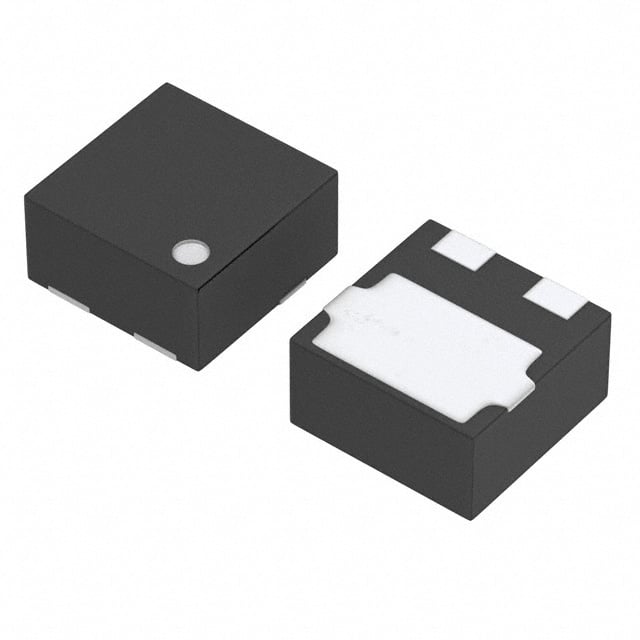
XC61GC1002HR-G is available in a surface mount package.
Essence
The essence of XC61GC1002HR-G lies in its ability to provide accurate voltage regulation in electronic circuits.
Packaging/Quantity
XC61GC1002HR-G is typically packaged in reels or tubes, with varying quantities depending on the supplier.
Specifications
- Input Voltage Range: 1.8V - 6.0V
- Output Voltage: 1.0V
- Output Current: 100mA
- Dropout Voltage: 0.3V (typical)
- Quiescent Current: 30μA (typical)
- Operating Temperature Range: -40°C to +85°C
Detailed Pin Configuration
XC61GC1002HR-G has three pins:
- VIN: Input voltage pin
- VOUT: Output voltage pin
- GND: Ground pin
Functional Features
- Voltage regulation: XC61GC1002HR-G ensures a stable output voltage regardless of input voltage fluctuations.
- Low dropout voltage: It operates efficiently even when the input voltage is close to the desired output voltage.
- Low quiescent current: The device consumes minimal power when not actively regulating the voltage.
Advantages and Disadvantages
Advantages
- Compact size allows for easy integration into small electronic devices.
- High precision ensures accurate voltage regulation.
- Low power consumption prolongs battery life in portable devices.
- Wide operating temperature range makes it suitable for various environments.
Disadvantages
- Limited output current may not be suitable for high-power applications.
- Dropout voltage may cause a slight decrease in efficiency.
Working Principles
XC61GC1002HR-G utilizes a voltage reference and feedback mechanism to maintain a constant output voltage. It compares the output voltage with a reference voltage and adjusts the internal circuitry accordingly to regulate the output voltage.
Detailed Application Field Plans
XC61GC1002HR-G finds applications in various electronic devices, including but not limited to: - Mobile phones - Portable media players - Digital cameras - Wearable devices - IoT devices
Detailed and Complete Alternative Models
Some alternative models that can be considered as alternatives to XC61GC1002HR-G are: - XC61CC1002MR-G - XC61DC1002NR-G - XC61EC1002PR-G - XC61FC1002SR-G
These models offer similar functionality and characteristics, providing options for different design requirements.
Word count: 346 words
Énumérez 10 questions et réponses courantes liées à l'application de XC61GC1002HR-G dans les solutions techniques
Sure! Here are 10 common questions and answers related to the application of XC61GC1002HR-G in technical solutions:
Question: What is XC61GC1002HR-G?
Answer: XC61GC1002HR-G is a voltage detector IC (integrated circuit) manufactured by Torex Semiconductor. It is commonly used for detecting and monitoring voltage levels in various electronic applications.Question: What is the operating voltage range of XC61GC1002HR-G?
Answer: The operating voltage range of XC61GC1002HR-G is typically between 0.8V and 6.0V.Question: How does XC61GC1002HR-G work?
Answer: XC61GC1002HR-G works by comparing the input voltage with a fixed reference voltage. When the input voltage exceeds the reference voltage, the output of the IC changes state, indicating a voltage detection event.Question: What is the output configuration of XC61GC1002HR-G?
Answer: XC61GC1002HR-G has an open-drain output configuration, which means it can sink current but cannot source current. An external pull-up resistor is required to provide the output voltage level.Question: What is the typical quiescent current consumption of XC61GC1002HR-G?
Answer: The typical quiescent current consumption of XC61GC1002HR-G is very low, usually around 1.0µA, making it suitable for battery-powered applications.Question: Can XC61GC1002HR-G be used as an overvoltage protection device?
Answer: No, XC61GC1002HR-G is primarily designed as a voltage detection device and not as an overvoltage protection device. It is recommended to use dedicated overvoltage protection circuits in critical applications.Question: What is the response time of XC61GC1002HR-G?
Answer: The response time of XC61GC1002HR-G is typically very fast, usually within a few microseconds, allowing for quick detection and response to voltage changes.Question: Can XC61GC1002HR-G be used in automotive applications?
Answer: Yes, XC61GC1002HR-G is suitable for automotive applications as it meets the AEC-Q100 automotive qualification standards.Question: Is XC61GC1002HR-G available in different package options?
Answer: Yes, XC61GC1002HR-G is available in various package options, including SOT-23, SOT-89, and USP-4B.Question: Are there any specific precautions or considerations when using XC61GC1002HR-G?
Answer: It is important to ensure proper decoupling and filtering of the power supply to minimize noise interference. Additionally, attention should be given to the maximum voltage rating and temperature limits specified in the datasheet to avoid damaging the IC.