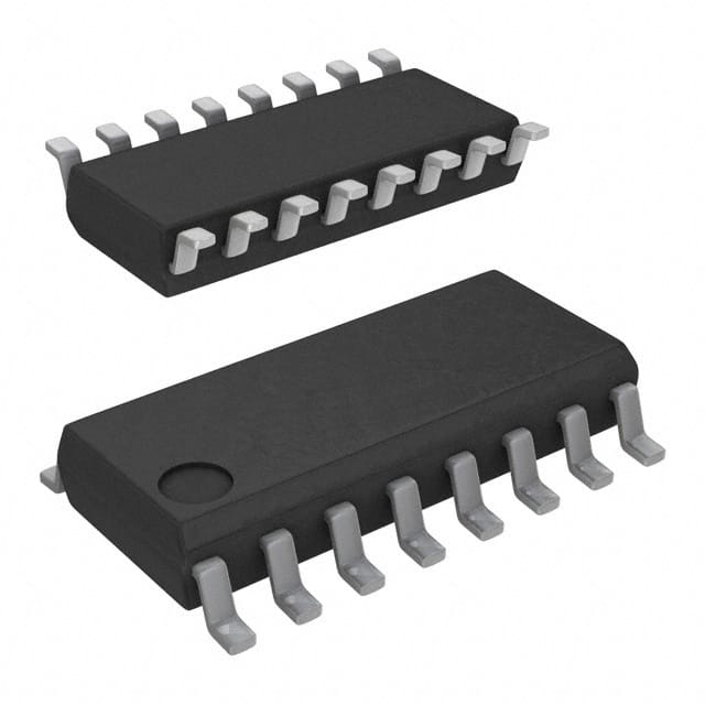
Voir les spécifications pour les détails du produit.

TLV5627IDG4
Product Overview
- Category: Integrated Circuit (IC)
- Use: Digital-to-Analog Converter (DAC)
- Characteristics: High-speed, low-power consumption
- Package: 8-pin SOIC (Small Outline Integrated Circuit)
- Essence: Converts digital signals into analog voltages
- Packaging/Quantity: Tape and reel packaging, 2500 units per reel
Specifications
- Resolution: 12 bits
- Number of Channels: 1
- Output Type: Voltage
- Supply Voltage: 2.7V to 5.5V
- Operating Temperature Range: -40°C to +85°C
- Conversion Rate: 400 kSPS (Samples per Second)
- Interface: Serial SPI (Serial Peripheral Interface)
Pin Configuration
The TLV5627IDG4 has the following pin configuration:
```
| | --| VDD |-- --| GND |-- --| DIN |-- --| CS |-- --| SCLK |-- --| LDAC |-- --| OUT |-- |___________| ```
- VDD: Power supply voltage
- GND: Ground reference
- DIN: Serial data input
- CS: Chip select input
- SCLK: Serial clock input
- LDAC: Load DAC input
- OUT: Analog output voltage
Functional Features
- High-speed conversion with a sampling rate of 400 kSPS
- Low power consumption for energy-efficient operation
- Single-channel DAC with 12-bit resolution for precise analog output
- Serial SPI interface for easy integration with microcontrollers or other digital devices
- Load DAC input allows simultaneous update of multiple DACs
Advantages and Disadvantages
Advantages
- High-speed conversion enables real-time applications
- Low power consumption extends battery life in portable devices
- Compact 8-pin package saves board space
- Serial interface simplifies communication with digital systems
Disadvantages
- Limited to single-channel output
- Requires an external voltage reference for accurate analog output
Working Principles
The TLV5627IDG4 is a digital-to-analog converter that converts digital signals into corresponding analog voltages. It utilizes a 12-bit resolution to provide precise analog outputs. The device operates on a supply voltage ranging from 2.7V to 5.5V and communicates with external systems through a serial SPI interface.
To convert digital data into analog voltages, the TLV5627IDG4 receives serial data input (DIN) and clock input (SCLK) signals. The chip select input (CS) enables or disables the device for communication. The load DAC input (LDAC) allows simultaneous update of multiple DACs. The analog output voltage is provided at the OUT pin.
Detailed Application Field Plans
The TLV5627IDG4 can be used in various applications, including:
- Audio Systems: Providing analog audio signals for amplifiers, speakers, and headphones.
- Industrial Automation: Generating control signals for motor speed control, valve positioning, and process control.
- Test and Measurement Equipment: Producing precise analog signals for signal generation and calibration.
- Communication Systems: Generating analog signals for modulation and demodulation processes.
- Instrumentation: Converting digital sensor readings into analog signals for measurement and control.
Detailed and Complete Alternative Models
Some alternative models to the TLV5627IDG4 are:
- MCP4921: 12-bit DAC with SPI interface and voltage output.
- MAX5216: 16-bit DAC with SPI interface and current output.
- AD5662: 16-bit DAC with I2C interface and voltage output.
- DAC0808: 8-bit DAC with parallel interface and voltage output.
These alternative models offer different resolutions, interfaces, and output types to suit specific application requirements.
Word count: 452 words
Énumérez 10 questions et réponses courantes liées à l'application de TLV5627IDG4 dans les solutions techniques
Sure! Here are 10 common questions and answers related to the application of TLV5627IDG4:
Q: What is TLV5627IDG4? A: TLV5627IDG4 is a digital-to-analog converter (DAC) chip manufactured by Texas Instruments.
Q: What is the resolution of TLV5627IDG4? A: TLV5627IDG4 has a resolution of 8 bits, meaning it can convert digital values into analog signals with 256 possible levels.
Q: What is the supply voltage range for TLV5627IDG4? A: The supply voltage range for TLV5627IDG4 is typically between 2.7V and 5.5V.
Q: Can TLV5627IDG4 be used in both single-ended and differential output configurations? A: Yes, TLV5627IDG4 can be used in both single-ended and differential output configurations, providing flexibility in various applications.
Q: What is the maximum settling time of TLV5627IDG4? A: The maximum settling time of TLV5627IDG4 is typically 10µs, ensuring fast and accurate conversion.
Q: Does TLV5627IDG4 have an internal reference voltage? A: No, TLV5627IDG4 does not have an internal reference voltage. An external reference voltage must be provided for proper operation.
Q: Can TLV5627IDG4 operate in a temperature range outside the industrial range? A: TLV5627IDG4 is designed to operate within the industrial temperature range of -40°C to +85°C. Operating outside this range may affect its performance.
Q: What is the power consumption of TLV5627IDG4? A: The power consumption of TLV5627IDG4 depends on various factors such as supply voltage and output load, but it typically ranges from 0.5mW to 2mW.
Q: Can TLV5627IDG4 be used in battery-powered applications? A: Yes, TLV5627IDG4 can be used in battery-powered applications due to its low power consumption and wide supply voltage range.
Q: Are there any evaluation boards or reference designs available for TLV5627IDG4? A: Yes, Texas Instruments provides evaluation boards and reference designs for TLV5627IDG4, which can help users quickly prototype and integrate the chip into their applications.
Please note that these answers are general and may vary depending on specific application requirements and datasheet specifications.

