

Voir les spécifications pour les détails du produit.
THS4502IDGN
Product Overview
- Category: Integrated Circuit (IC)
- Use: Amplifier
- Characteristics: High-speed, low-power, rail-to-rail output
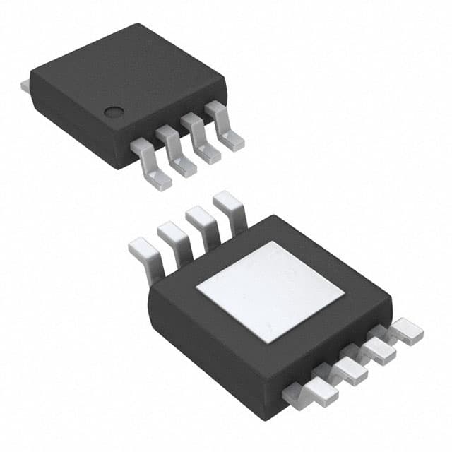
- Package: 8-pin MSOP (Mini Small Outline Package)
- Essence: The THS4502IDGN is a high-speed amplifier IC designed for various applications requiring precision signal amplification.
- Packaging/Quantity: Available in reels of 2500 units
Specifications
- Supply Voltage: ±2.5V to ±6V
- Input Offset Voltage: ±1mV
- Gain Bandwidth Product: 500MHz
- Slew Rate: 1800V/µs
- Input Bias Current: ±1nA
- Operating Temperature Range: -40°C to +85°C
Pin Configuration
The THS4502IDGN has the following pin configuration:
```
| | --| V- OUT |-- Pin 1: Negative Power Supply (V-) --| IN+ VCC |-- Pin 2: Positive Power Supply (VCC) --| IN- GND |-- Pin 3: Ground (GND) --| V+ NC |-- Pin 4: Not Connected (NC) --| NC IN- |-- Pin 5: Inverting Input (-) --| NC IN+ |-- Pin 6: Non-Inverting Input (+) --| OUT V- |-- Pin 7: Output (OUT) --| VCC V+ |-- Pin 8: Positive Power Supply (V+) |___________| ```
Functional Features
- High-speed amplification with a gain bandwidth product of 500MHz
- Rail-to-rail output swing capability
- Low-power consumption
- Wide operating temperature range (-40°C to +85°C)
- Low input offset voltage for accurate signal amplification
Advantages and Disadvantages
Advantages
- High-speed performance suitable for various applications
- Rail-to-rail output allows for maximum utilization of the supply voltage range
- Low-power consumption extends battery life in portable devices
- Wide operating temperature range enables usage in extreme environments
- Low input offset voltage ensures precise signal amplification
Disadvantages
- Limited availability in alternative packages
- May require additional external components for specific applications
Working Principles
The THS4502IDGN is a high-speed amplifier that operates by amplifying the input signal with high gain and providing a rail-to-rail output swing. It utilizes a differential input stage to achieve low input offset voltage and high common-mode rejection ratio. The amplifier's internal circuitry is designed to minimize power consumption while maintaining high-speed performance.
Detailed Application Field Plans
The THS4502IDGN is commonly used in the following applications:
- Audio amplification in portable devices such as smartphones and tablets
- Signal conditioning in medical equipment like ECG monitors
- Video signal amplification in professional broadcasting equipment
- Data acquisition systems requiring high-speed amplification
- Industrial control systems for precise signal processing
Alternative Models
Below are some alternative models that can be considered:
- AD8052ARZ: Dual, high-speed amplifier with rail-to-rail output
- LMH6629MA/NOPB: Ultra-low noise, high-speed amplifier with rail-to-rail output
- MAX4194ESA+: Precision, high-speed amplifier with low input offset voltage
These alternative models offer similar functionality and can be used as substitutes depending on specific requirements.
Word count: 346 words
Énumérez 10 questions et réponses courantes liées à l'application de THS4502IDGN dans les solutions techniques
Sure! Here are 10 common questions and answers related to the application of THS4502IDGN in technical solutions:
Question: What is THS4502IDGN?
- Answer: THS4502IDGN is a high-speed operational amplifier (op-amp) designed for various applications in technical solutions.Question: What is the voltage supply range for THS4502IDGN?
- Answer: The voltage supply range for THS4502IDGN is typically between ±2.25V and ±6V.Question: What is the bandwidth of THS4502IDGN?
- Answer: THS4502IDGN has a bandwidth of 500MHz, making it suitable for high-frequency applications.Question: Can THS4502IDGN be used in audio applications?
- Answer: Yes, THS4502IDGN can be used in audio applications such as audio amplifiers or audio signal processing.Question: Is THS4502IDGN suitable for low-power applications?
- Answer: No, THS4502IDGN is not specifically designed for low-power applications. It is more suitable for high-speed and high-performance applications.Question: What is the input voltage noise of THS4502IDGN?
- Answer: The input voltage noise of THS4502IDGN is typically around 3.9nV/√Hz, which ensures good signal integrity.Question: Can THS4502IDGN operate in a single-supply configuration?
- Answer: Yes, THS4502IDGN can operate in a single-supply configuration, but it requires proper biasing and level shifting for the input and output signals.Question: What is the maximum output current of THS4502IDGN?
- Answer: The maximum output current of THS4502IDGN is typically around 100mA, allowing it to drive various loads.Question: Can THS4502IDGN be used in high-gain applications?
- Answer: Yes, THS4502IDGN has a high open-loop gain, making it suitable for high-gain applications such as instrumentation amplifiers.Question: Is THS4502IDGN available in different package options?
- Answer: Yes, THS4502IDGN is available in different package options, including the 8-pin SOIC and 8-pin VSSOP packages.
Please note that the answers provided here are general and may vary depending on specific datasheet specifications or application requirements.