

Voir les spécifications pour les détails du produit.
SN75LVDS388ADBT
Product Overview
- Category: Integrated Circuit (IC)
- Use: LVDS Serializer/Deserializer
- Characteristics:
- High-speed data transmission
- Low voltage differential signaling
- Robust noise immunity
- Compact package size
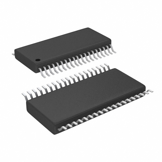
- Package: TSSOP-48
- Essence: Converts parallel data to serial data and vice versa using LVDS technology
- Packaging/Quantity: Tape and reel, 2500 units per reel
Specifications
- Supply Voltage Range: 3.0V to 3.6V
- Operating Temperature Range: -40°C to +85°C
- Data Rate: Up to 400 Mbps
- Number of Channels: 8
- Input/Output Interface: LVCMOS/LVTTL
- ESD Protection: ±8kV HBM, ±15kV IEC61000-4-2 Air-Gap Discharge, ±8kV IEC61000-4-2 Contact Discharge
Pin Configuration
The SN75LVDS388ADBT has a total of 48 pins. The pin configuration is as follows:
- VCCO
- GND
- Q0
- Q1
- Q2
- Q3
- Q4
- Q5
- Q6
- Q7
- Q8
- Q9
- Q10
- Q11
- Q12
- Q13
- Q14
- Q15
- Q16
- Q17
- Q18
- Q19
- Q20
- Q21
- Q22
- Q23
- Q24
- Q25
- Q26
- Q27
- Q28
- Q29
- Q30
- Q31
- GND
- VCCO
- CLKIN
- CLKSEL
- GND
- VCCO
- OE#
- GND
- VCCO
- LVDS_OUT
- GND
- VCCO
- LVDS_IN
- GND
Functional Features
- Converts parallel data to serial data and vice versa
- Supports high-speed data transmission up to 400 Mbps
- Utilizes Low Voltage Differential Signaling (LVDS) technology for noise immunity
- Provides 8 channels for data transmission
- Offers LVCMOS/LVTTL compatible input/output interface
- Includes built-in ESD protection for enhanced reliability
Advantages and Disadvantages
Advantages: - High-speed data transmission capability - Robust noise immunity due to LVDS technology - Compact package size for space-constrained applications - Wide supply voltage range for flexibility
Disadvantages: - Requires LVCMOS/LVTTL level shifting for interfacing with other logic families - Limited number of channels compared to some alternative models
Working Principles
The SN75LVDS388ADBT operates by converting parallel data into serial data using LVDS technology. It receives parallel data through its input pins and converts it into a serial stream of LVDS-encoded data. Similarly, it can receive a serial stream of LVDS-encoded data and convert it back into parallel data.
The LVDS technology used in the IC allows for high-speed data transmission while providing robust noise immunity. LVDS utilizes differential signaling, where data is transmitted as a voltage difference between two lines, reducing the impact of common-mode noise.
Detailed Application Field Plans
The SN75LVDS388ADBT is commonly used in various applications that require high-speed data transmission with noise immunity. Some of the typical application fields include:
- Display Technology: The IC can be used in LCD monitors, televisions, and digital signage displays to transmit video data from the source to the display panel.
- Industrial Automation: It finds applications in industrial control systems, PLCs (Programmable Logic Controllers), and robotics, where reliable and high-speed data transmission is crucial.
- Automotive Electronics: The IC can be utilized in automotive infotainment systems, instrument clusters, and advanced driver-assistance systems (ADAS) for transmitting data between different components.
- Communication Systems: It can be employed in high-speed communication interfaces such as Ethernet switches, routers, and optical transceivers to ensure efficient data transfer.
Detailed and Complete Alternative Models
Some alternative models to SN75LVDS388ADBT that offer similar functionality are:
- SN65LVDS389DBT
- DS90LV048ATMTC
- MAX9126ESE+
- ADN4650BRZ
- MC100EP16VSDTG
Énumérez 10 questions et réponses courantes liées à l'application de SN75LVDS388ADBT dans les solutions techniques
Sure! Here are 10 common questions and answers related to the application of SN75LVDS388ADBT in technical solutions:
Q: What is SN75LVDS388ADBT? A: SN75LVDS388ADBT is a high-speed differential line driver and receiver specifically designed for LVDS (Low Voltage Differential Signaling) applications.
Q: What are the key features of SN75LVDS388ADBT? A: Some key features of SN75LVDS388ADBT include low power consumption, wide operating voltage range, high data rates, and compatibility with LVDS standards.
Q: What is the typical application of SN75LVDS388ADBT? A: SN75LVDS388ADBT is commonly used in applications that require high-speed data transmission over long distances, such as in video surveillance systems, automotive infotainment, and industrial automation.
Q: How does SN75LVDS388ADBT achieve high-speed data transmission? A: SN75LVDS388ADBT uses LVDS technology, which employs differential signaling to transmit data at high speeds while minimizing noise and power consumption.
Q: What is the maximum data rate supported by SN75LVDS388ADBT? A: SN75LVDS388ADBT supports data rates up to 400 Mbps, making it suitable for various high-speed communication protocols.
Q: Can SN75LVDS388ADBT be used in both transmitter and receiver applications? A: Yes, SN75LVDS388ADBT can be used as both a line driver (transmitter) and a line receiver, providing flexibility in system design.
Q: Does SN75LVDS388ADBT require external components for operation? A: Yes, SN75LVDS388ADBT requires external termination resistors and capacitors to ensure proper signal integrity and impedance matching.
Q: What is the operating voltage range of SN75LVDS388ADBT? A: SN75LVDS388ADBT operates from a supply voltage range of 3.0V to 3.6V, making it compatible with common power supply levels.
Q: Can SN75LVDS388ADBT tolerate electrostatic discharge (ESD)? A: Yes, SN75LVDS388ADBT has built-in ESD protection, typically rated for up to ±8kV contact discharge and ±15kV air discharge.
Q: Is SN75LVDS388ADBT available in different package options? A: Yes, SN75LVDS388ADBT is available in various package options, such as TSSOP and QFN, allowing for easy integration into different PCB layouts.
Please note that these answers are general and may vary depending on the specific application and requirements. It's always recommended to refer to the datasheet and consult the manufacturer for detailed information.