

Voir les spécifications pour les détails du produit.
SN74SSTV16859DGGR
Product Overview
Category
The SN74SSTV16859DGGR belongs to the category of integrated circuits (ICs).
Use
This IC is commonly used in electronic devices for signal transmission and processing.
Characteristics
- High-speed operation
- Low power consumption
- Wide operating voltage range
- Robust design for reliable performance
Package
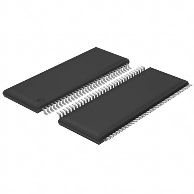
The SN74SSTV16859DGGR is available in a small form factor package, such as a 56-pin TSSOP (Thin Shrink Small Outline Package).
Essence
The essence of this product lies in its ability to efficiently transmit and process signals in electronic systems.
Packaging/Quantity
The SN74SSTV16859DGGR is typically packaged in reels or tubes, with a quantity of around 2500 units per reel/tube.
Specifications
- Supply Voltage: 2.3V to 3.6V
- Operating Temperature Range: -40°C to +85°C
- Input/Output Type: Differential
- Number of Channels: 20
- Data Rate: Up to 1.6 Gbps
- Logic Family: SSTL_18
Detailed Pin Configuration
The pin configuration of SN74SSTV16859DGGR is as follows:
Pin 1: VCC
Pin 2: GND
Pin 3: Channel 1 Data Input (D0+)
Pin 4: Channel 1 Data Input (D0-)
...
Pin 55: Channel 20 Data Output (Q19+)
Pin 56: Channel 20 Data Output (Q19-)
Functional Features
- High-speed data transmission
- Low power consumption
- Built-in ESD protection
- Compatible with various logic families
- Supports hot-plugging capability
Advantages and Disadvantages
Advantages
- High-speed operation enables efficient signal transmission.
- Low power consumption contributes to energy efficiency.
- Robust design ensures reliable performance even in challenging environments.
- Wide operating voltage range allows compatibility with different systems.
Disadvantages
- Limited number of channels compared to some other ICs in the same category.
- May require additional external components for certain applications.
Working Principles
The SN74SSTV16859DGGR operates based on differential signaling principles. It receives input signals through its data input pins, processes them internally, and provides the processed output signals through its data output pins. The IC utilizes advanced circuitry to achieve high-speed data transmission while minimizing power consumption.
Detailed Application Field Plans
The SN74SSTV16859DGGR finds applications in various fields, including:
- Telecommunications: Used in high-speed data communication systems, such as fiber optic networks.
- Computer Networking: Employed in routers, switches, and network interface cards for efficient data transmission.
- Consumer Electronics: Integrated into devices like high-definition televisions and gaming consoles for signal processing.
- Automotive Electronics: Utilized in automotive infotainment systems and advanced driver-assistance systems (ADAS) for reliable signal transmission.
Detailed and Complete Alternative Models
Some alternative models that offer similar functionality to SN74SSTV16859DGGR are:
- SN65LVDS179DGGR
- SN65LVDS180DGGR
- SN65LVDS182DGGR
- SN65LVDS184DGGR
These alternative models belong to the same category of ICs and provide comparable features and specifications.
Word count: 530 words
Énumérez 10 questions et réponses courantes liées à l'application de SN74SSTV16859DGGR dans les solutions techniques
Sure! Here are 10 common questions and answers related to the application of SN74SSTV16859DGGR in technical solutions:
Q: What is SN74SSTV16859DGGR? A: SN74SSTV16859DGGR is a high-speed, 16-bit universal bus driver and receiver designed for applications requiring high-performance transmission of signals over long distances.
Q: What are the key features of SN74SSTV16859DGGR? A: Some key features include wide voltage range operation, low power consumption, high-speed data transmission, and compatibility with various logic families.
Q: What is the maximum operating frequency of SN74SSTV16859DGGR? A: The maximum operating frequency of SN74SSTV16859DGGR is typically around 200 MHz.
Q: Can SN74SSTV16859DGGR be used as a bidirectional buffer? A: Yes, SN74SSTV16859DGGR can be used as a bidirectional buffer, allowing data to flow in both directions on the bus.
Q: What is the voltage supply range for SN74SSTV16859DGGR? A: SN74SSTV16859DGGR operates within a voltage supply range of 2.3V to 3.6V.
Q: Is SN74SSTV16859DGGR compatible with TTL and CMOS logic levels? A: Yes, SN74SSTV16859DGGR is compatible with both TTL and CMOS logic levels, making it versatile for use in various systems.
Q: Can SN74SSTV16859DGGR handle hot-swapping of devices? A: Yes, SN74SSTV16859DGGR has built-in hot-swapping protection, allowing for safe insertion and removal of devices while the system is powered.
Q: What is the output drive strength of SN74SSTV16859DGGR? A: SN74SSTV16859DGGR has a strong output drive capability, typically around 24 mA, ensuring reliable signal transmission.
Q: Does SN74SSTV16859DGGR support bus hold functionality? A: Yes, SN74SSTV16859DGGR supports bus hold functionality, which helps to maintain the last valid logic state on the outputs during bus transitions.
Q: Can SN74SSTV16859DGGR be used in high-speed data communication applications? A: Absolutely! SN74SSTV16859DGGR is specifically designed for high-speed data transmission, making it suitable for applications such as networking, telecommunications, and data centers.
Please note that these answers are general and may vary depending on specific datasheet specifications and application requirements.