

Voir les spécifications pour les détails du produit.
SN74LVTH182652APM
Product Overview
- Category: Integrated Circuit
- Use: Logic Level Translator
- Characteristics: Low Voltage, High-Speed, 18-Bit Bus Transceiver
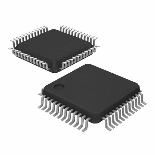
- Package: 56-Terminal BGA (Ball Grid Array)
- Essence: Translates signals between different voltage levels in digital systems
- Packaging/Quantity: Tape and Reel, 250 units per reel
Specifications
- Supply Voltage Range: 1.65V to 3.6V
- Input Voltage Range: 0V to VCC
- Output Voltage Range: 0V to VCC
- Operating Temperature Range: -40°C to +85°C
- Propagation Delay Time: 2.5ns (Max)
- Output Drive Strength: ±12mA
- ESD Protection: >2000V
Detailed Pin Configuration
The SN74LVTH182652APM has a total of 56 pins. The pin configuration is as follows:
- A1
- Y1
- GND
- Y2
- A2
- GND
- B1
- Y3
- GND
- Y4
- B2
- GND
- A3
- Y5
- GND
- Y6
- A4
- GND
- B3
- Y7
- GND
- Y8
- B4
- GND
- A5
- Y9
- GND
- Y10
- A6
- GND
- B5
- Y11
- GND
- Y12
- B6
- GND
- A7
- Y13
- GND
- Y14
- A8
- GND
- B7
- Y15
- GND
- Y16
- B8
- GND
- VCCB
- OEAB
- GND
- OEBA
- VCCA
- GND
- GND
- VCC
Functional Features
- Bidirectional voltage translation between two independent buses
- Supports mixed-mode signal operation on each port
- 3-state outputs for bus isolation
- Low power consumption
- High-speed operation
Advantages and Disadvantages
Advantages: - Wide supply voltage range allows compatibility with various systems - Fast propagation delay time enables high-speed data transmission - 3-state outputs provide flexibility in bus control
Disadvantages: - Limited number of input/output channels (18-bit) - Requires careful consideration of voltage levels to avoid signal distortion
Working Principles
The SN74LVTH182652APM is a logic level translator designed to enable communication between digital systems operating at different voltage levels. It utilizes a combination of CMOS and TTL technologies to achieve bidirectional voltage translation.
The device consists of two 18-bit bus transceivers, which can operate independently. Each transceiver has separate control pins for output enable (OEAB and OEBA), allowing individual bus control. The inputs and outputs are compatible with both CMOS and TTL voltage levels.
When the output enable pin is active, the device enters a high-impedance state, isolating the bus from the rest of the system. This feature facilitates multi-master systems and prevents bus contention.
Detailed Application Field Plans
The SN74LVTH182652APM is commonly used in various applications where voltage translation is required. Some of the typical application fields include:
- Microcontrollers and microprocessors
- Memory interfaces
- Communication systems
- Industrial automation
- Automotive electronics
Detailed and Complete Alternative Models
- SN74LVC1T45DBVR: Single-Bit Dual-Supply Bus Transceiver
- SN74AVC4T245PW: 4-Bit Dual-Supply Bus Transceiver
- SN74HCT125N: Quad Bus Buffer Gate with 3-State Outputs
- SN74LVCH16244ADGGR: 16-Bit Bus Transceiver with 3-State Outputs
- SN74LVC8T245PWR: 8-Bit Dual-Supply Bus Transceiver
These alternative models offer similar functionality and can be considered as substitutes for the SN74LVTH182652APM in different applications.
Word count: 536 words
Énumérez 10 questions et réponses courantes liées à l'application de SN74LVTH182652APM dans les solutions techniques
Sure! Here are 10 common questions and answers related to the application of SN74LVTH182652APM:
Q: What is SN74LVTH182652APM? A: SN74LVTH182652APM is a specific type of integrated circuit (IC) that functions as a 18-bit universal bus transceiver with 3-state outputs.
Q: What is the purpose of SN74LVTH182652APM? A: The purpose of this IC is to enable bidirectional data transfer between two buses with different voltage levels, while providing isolation when needed.
Q: What voltage levels does SN74LVTH182652APM support? A: SN74LVTH182652APM supports voltage levels ranging from 1.65V to 3.6V, making it compatible with various logic families.
Q: How many bits can SN74LVTH182652APM handle? A: This IC can handle 18 bits of data, allowing for the transmission of large amounts of information.
Q: Can SN74LVTH182652APM be used in both input and output applications? A: Yes, SN74LVTH182652APM can be used as both an input and output buffer, making it versatile in different technical solutions.
Q: Does SN74LVTH182652APM have built-in protection features? A: Yes, this IC has built-in ESD (electrostatic discharge) protection, which helps safeguard against damage caused by static electricity.
Q: What is the maximum operating frequency of SN74LVTH182652APM? A: SN74LVTH182652APM has a maximum operating frequency of 200 MHz, allowing for high-speed data transmission.
Q: Can SN74LVTH182652APM be used in automotive applications? A: Yes, SN74LVTH182652APM is suitable for automotive applications as it meets the necessary requirements for temperature range and reliability.
Q: Does SN74LVTH182652APM support hot-swapping of devices? A: No, this IC does not support hot-swapping. It is recommended to power down the circuit before connecting or disconnecting devices.
Q: Are there any specific layout considerations when using SN74LVTH182652APM? A: Yes, it is important to follow the recommended layout guidelines provided in the datasheet to ensure proper signal integrity and minimize noise.
Please note that these answers are general and may vary depending on the specific application and requirements. Always refer to the datasheet and consult with technical experts for accurate information.