

Voir les spécifications pour les détails du produit.
SN74LVCC4245ADBRE4
Product Overview
Category
SN74LVCC4245ADBRE4 belongs to the category of integrated circuits (ICs).
Use
This IC is commonly used for voltage level shifting and signal buffering in various electronic applications.
Characteristics
- Low-voltage operation: The SN74LVCC4245ADBRE4 operates at a low voltage, making it suitable for battery-powered devices.
- Bidirectional voltage translation: It allows bidirectional voltage translation between different logic levels.
- High-speed performance: This IC offers high-speed data transmission, enabling efficient signal processing.
- ESD protection: It provides built-in electrostatic discharge (ESD) protection, ensuring reliability in harsh environments.
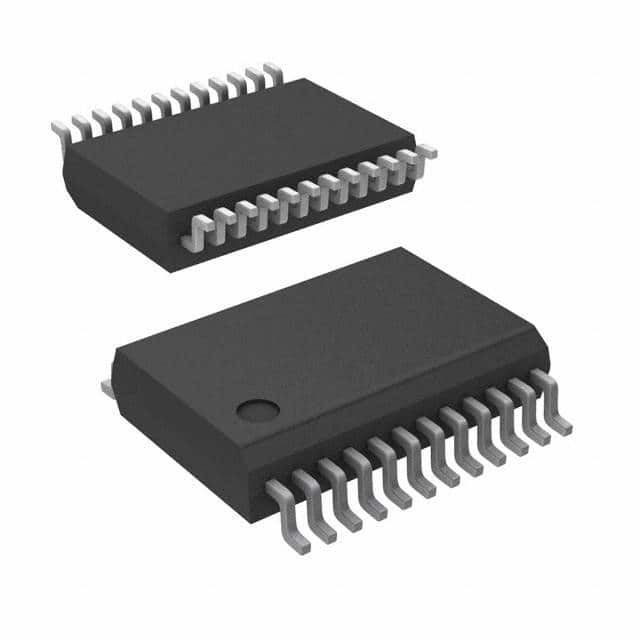
Package
The SN74LVCC4245ADBRE4 is available in a small-sized package, which is easy to handle and mount on printed circuit boards (PCBs).
Essence
The essence of SN74LVCC4245ADBRE4 lies in its ability to facilitate voltage level shifting and signal buffering, ensuring seamless communication between different logic levels.
Packaging/Quantity
This IC is typically packaged in reels or tubes, with a quantity of 2500 units per reel/tube.
Specifications
- Supply Voltage Range: 1.65V to 5.5V
- Logic Family: LVCC
- Number of Channels: 8
- Input/Output Type: Bidirectional
- Operating Temperature Range: -40°C to +85°C
- Propagation Delay Time: 6 ns (max)
- Output Current: ±12 mA
Detailed Pin Configuration
The SN74LVCC4245ADBRE4 has a total of 24 pins, which are assigned as follows:
- OE (Output Enable) 1
- A1 (Channel Select) 1
- I/O1 (Bidirectional I/O) 1
- GND (Ground)
- I/O2 (Bidirectional I/O) 2
- A2 (Channel Select) 2
- OE (Output Enable) 2
- VCC (Supply Voltage)
- I/O3 (Bidirectional I/O) 3
- A3 (Channel Select) 3
- I/O4 (Bidirectional I/O) 4
- GND (Ground)
- I/O5 (Bidirectional I/O) 5
- A4 (Channel Select) 4
- OE (Output Enable) 3
- VCC (Supply Voltage)
- I/O6 (Bidirectional I/O) 6
- A5 (Channel Select) 5
- I/O7 (Bidirectional I/O) 7
- GND (Ground)
- I/O8 (Bidirectional I/O) 8
- A6 (Channel Select) 6
- OE (Output Enable) 4
- VCC (Supply Voltage)
Functional Features
- Bidirectional voltage translation: The SN74LVCC4245ADBRE4 allows bidirectional voltage translation between different logic levels, enabling seamless communication between devices operating at different voltages.
- Output enable control: The output enable pins (OE) provide control over the direction of data flow, allowing the user to enable or disable the IC's output.
- Channel selection: The channel select pins (A1-A6) determine which input/output channels are active, providing flexibility in routing signals.
Advantages and Disadvantages
Advantages
- Low-voltage operation makes it suitable for battery-powered devices.
- High-speed performance enables efficient signal processing.
- Built-in ESD protection ensures reliability in harsh environments.
- Bidirectional voltage translation simplifies interfacing between different logic levels.
Disadvantages
- Limited number of channels (8) may not be sufficient for complex applications requiring a higher channel count.
- Propagation delay time (6 ns) may introduce latency in time-critical applications.
Working Principles
The SN74LVCC4245ADBRE4 operates based on the principles of voltage level shifting and signal buffering. It utilizes a combination of transistors, resistors, and capacitors to achieve bidirectional voltage translation between different logic levels. The output enable pins control the direction of data flow, while the channel select pins determine which input/output channels are active.
Detailed Application Field Plans
The SN74LVCC4245ADBRE4 finds applications in various fields, including:
- Consumer Electronics: Used in smartphones, tablets, and portable media players for voltage level shifting and signal buffering.
- Industrial Automation: Employed in PLCs (Programmable Logic Controllers) and industrial control systems for interfacing between different voltage domains.
- Automotive Electronics: Utilized in automotive infotainment systems and ECU (Engine Control Unit) modules
Énumérez 10 questions et réponses courantes liées à l'application de SN74LVCC4245ADBRE4 dans les solutions techniques
Sure! Here are 10 common questions and answers related to the application of SN74LVCC4245ADBRE4 in technical solutions:
Q: What is SN74LVCC4245ADBRE4? A: SN74LVCC4245ADBRE4 is a bidirectional voltage level translator and voltage-level shifter integrated circuit (IC) manufactured by Texas Instruments.
Q: What is the purpose of SN74LVCC4245ADBRE4? A: SN74LVCC4245ADBRE4 is used to translate logic levels between different voltage domains, allowing communication between devices operating at different voltage levels.
Q: What voltage levels can SN74LVCC4245ADBRE4 handle? A: SN74LVCC4245ADBRE4 can handle voltage levels ranging from 1.65V to 5.5V.
Q: How many channels does SN74LVCC4245ADBRE4 have? A: SN74LVCC4245ADBRE4 has 8 bidirectional channels, allowing for simultaneous translation of up to 8 signals.
Q: Can SN74LVCC4245ADBRE4 be used for level shifting between different logic families? A: Yes, SN74LVCC4245ADBRE4 can be used for level shifting between various logic families such as TTL, CMOS, and LVTTL.
Q: What is the maximum data rate supported by SN74LVCC4245ADBRE4? A: SN74LVCC4245ADBRE4 supports a maximum data rate of 100 Mbps.
Q: Does SN74LVCC4245ADBRE4 require external pull-up or pull-down resistors? A: No, SN74LVCC4245ADBRE4 has built-in pull-up and pull-down resistors, eliminating the need for external components.
Q: Can SN74LVCC4245ADBRE4 be used in both 3.3V and 5V systems? A: Yes, SN74LVCC4245ADBRE4 is compatible with both 3.3V and 5V systems, making it versatile for various applications.
Q: Does SN74LVCC4245ADBRE4 have any built-in ESD protection? A: Yes, SN74LVCC4245ADBRE4 incorporates ESD protection on all pins, ensuring robustness against electrostatic discharge events.
Q: What package options are available for SN74LVCC4245ADBRE4? A: SN74LVCC4245ADBRE4 is available in a variety of package options, including SOIC (Small Outline Integrated Circuit) and TSSOP (Thin Shrink Small Outline Package).
Please note that these answers are general and may vary depending on specific application requirements.