

Voir les spécifications pour les détails du produit.
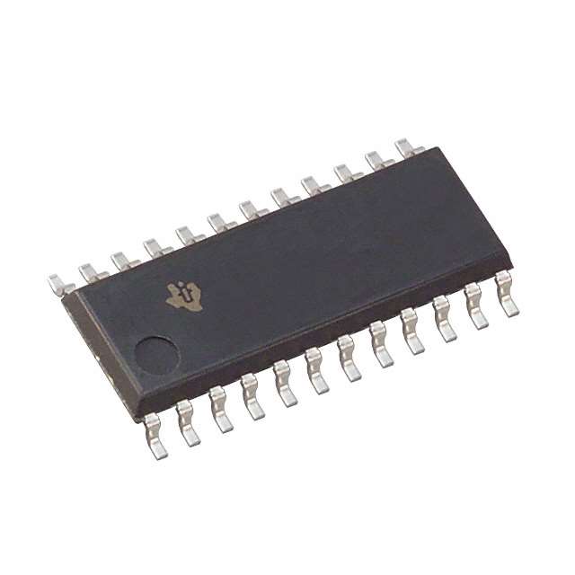
SN74LVC823ANSR
Product Overview
- Category: Integrated Circuit (IC)
- Use: Logic Level Shifter
- Characteristics: High-speed, low-voltage, CMOS technology
- Package: SOIC (Small Outline Integrated Circuit)
- Essence: Logic level shifting between different voltage domains
- Packaging/Quantity: Tape and Reel, 2500 units per reel
Specifications
- Supply Voltage Range: 1.65V to 3.6V
- Logic Voltage Levels: 1.8V and 3.3V
- Number of Inputs: 8
- Number of Outputs: 8
- Propagation Delay: 2.5ns (typical)
- Operating Temperature Range: -40°C to +85°C
Detailed Pin Configuration
The SN74LVC823ANSR has a total of 20 pins, which are assigned as follows:
- Pin 1: Output 1
- Pin 2: Input 1
- Pin 3: GND (Ground)
- Pin 4: Input 2
- Pin 5: Output 2
- Pin 6: Output 3
- Pin 7: Input 3
- Pin 8: VCC (Supply Voltage)
- Pin 9: Output 4
- Pin 10: Input 4
- Pin 11: Output 5
- Pin 12: Input 5
- Pin 13: Output 6
- Pin 14: Input 6
- Pin 15: Output 7
- Pin 16: Input 7
- Pin 17: Output 8
- Pin 18: Input 8
- Pin 19: GND (Ground)
- Pin 20: VCC (Supply Voltage)
Functional Features
- Logic level shifting between 1.8V and 3.3V voltage domains
- Bidirectional voltage translation
- High-speed operation
- Low power consumption
- ESD (Electrostatic Discharge) protection on all inputs and outputs
Advantages and Disadvantages
Advantages: - Enables communication between devices operating at different voltage levels - Fast propagation delay for quick signal transmission - Low power consumption for energy-efficient applications - ESD protection ensures robustness against electrostatic discharge
Disadvantages: - Limited to logic level shifting between 1.8V and 3.3V voltage domains - Not suitable for applications requiring level shifting beyond the specified voltage range
Working Principles
The SN74LVC823ANSR utilizes CMOS technology to perform logic level shifting. It consists of a combination of MOSFETs that act as switches, allowing signals to be translated between different voltage domains. The input signals are detected and amplified by the internal circuitry, which then drives the corresponding output pins with the appropriate voltage levels.
Detailed Application Field Plans
The SN74LVC823ANSR is commonly used in various applications where logic level shifting is required. Some of the typical application fields include:
- Microcontroller interfacing: The IC enables communication between microcontrollers operating at different voltage levels, facilitating data exchange and control.
- Sensor networks: It allows sensors with different voltage requirements to interface with a central processing unit, enabling seamless integration and data acquisition.
- Communication systems: The IC can be used in communication protocols that involve devices operating at different voltage domains, such as UART, SPI, or I2C interfaces.
- Battery-powered devices: Its low power consumption makes it suitable for portable electronic devices that rely on battery power, extending battery life.
Detailed and Complete Alternative Models
- TXS0108EPWR: Similar logic level shifter with 8 inputs and outputs, supporting voltage translation between 1.2V and 3.6V.
- SN74LVC4245APWR: Octal bus transceiver and level shifter with 8-bit bidirectional voltage translation between 1.2V and 5.5V.
- PCA9306DCUR: Dual bidirectional I2C-bus and SMBus voltage-level translator with automatic direction sensing.
These alternative models offer similar functionality to the SN74LVC823ANSR but may have different specifications or package options.
Word count: 510 words
Énumérez 10 questions et réponses courantes liées à l'application de SN74LVC823ANSR dans les solutions techniques
Sure! Here are 10 common questions and answers related to the application of SN74LVC823ANSR:
Q: What is SN74LVC823ANSR? A: SN74LVC823ANSR is a specific integrated circuit (IC) chip that belongs to the SN74LVC series of logic gates. It is an octal buffer/line driver with 3-state outputs.
Q: What is the purpose of SN74LVC823ANSR? A: SN74LVC823ANSR is used to provide buffering and line driving capabilities in digital circuits. It can be used to amplify signals, isolate different sections of a circuit, or interface between different voltage levels.
Q: What is the voltage range supported by SN74LVC823ANSR? A: SN74LVC823ANSR supports a wide voltage range, typically from 1.65V to 5.5V. This makes it compatible with various digital systems operating at different voltage levels.
Q: How many channels does SN74LVC823ANSR have? A: SN74LVC823ANSR has 8 channels, which means it can handle 8 separate input/output lines.
Q: What is the maximum output current of SN74LVC823ANSR? A: The maximum output current per channel of SN74LVC823ANSR is typically around 24mA, making it suitable for driving standard TTL or CMOS loads.
Q: Can SN74LVC823ANSR be used as a level shifter? A: Yes, SN74LVC823ANSR can be used as a level shifter since it can handle different voltage levels on its inputs and outputs. It allows interfacing between systems with different voltage requirements.
Q: Does SN74LVC823ANSR have built-in protection features? A: Yes, SN74LVC823ANSR has built-in ESD (electrostatic discharge) protection on its inputs and outputs, which helps safeguard the chip from damage due to static electricity.
Q: What is the propagation delay of SN74LVC823ANSR? A: The propagation delay of SN74LVC823ANSR is typically around 3.5ns, which means it takes approximately 3.5 nanoseconds for a signal to propagate through the chip.
Q: Can SN74LVC823ANSR be used in high-speed applications? A: Yes, SN74LVC823ANSR is designed for high-speed operation and can be used in applications where fast switching times are required.
Q: Are there any specific application notes or reference designs available for SN74LVC823ANSR? A: Yes, Texas Instruments, the manufacturer of SN74LVC823ANSR, provides application notes and reference designs that offer guidance on using the chip effectively in various technical solutions. These resources can be found on their website or obtained from their technical support team.