

Voir les spécifications pour les détails du produit.
SN74LVC2G08YZTR
Product Overview
- Category: Integrated Circuit (IC)
- Use: Logic Gate
- Characteristics: Dual 2-input AND gate
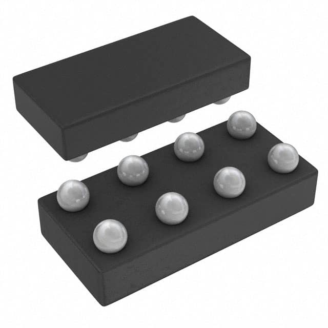
- Package: SOT-23-6
- Essence: High-speed CMOS technology
- Packaging/Quantity: Tape and Reel, 3000 pieces per reel
Specifications
- Supply Voltage Range: 1.65V to 5.5V
- High-Speed Operation: tpd = 3.8 ns (typ) at 3.3V
- Low Power Consumption: ICC = 1 µA (max) at TA = 25°C
- Schmitt-Trigger Inputs for Noise Immunity
- ESD Protection Exceeds JESD 22
Detailed Pin Configuration
The SN74LVC2G08YZTR has a total of 6 pins arranged as follows:
____
   1 |o    |
   2 |     |
   3 |     |
   4 |     |
   5 |     |
   6 |____o|
Pin Description: 1. A Input 1 2. B Input 2 3. Y Output 4. GND Ground 5. NC No Connection 6. VCC Supply Voltage
Functional Features
- Dual 2-input AND gate with Schmitt-trigger inputs
- High-speed operation allows for quick signal processing
- Low power consumption ensures energy efficiency
- Noise immunity provided by Schmitt-trigger inputs
- ESD protection exceeds industry standards, ensuring robustness
Advantages and Disadvantages
Advantages: - High-speed operation enables fast data processing - Low power consumption reduces energy usage - Schmitt-trigger inputs provide noise immunity - ESD protection ensures reliability in harsh environments
Disadvantages: - Limited to dual 2-input AND gate functionality - Not suitable for applications requiring more complex logic operations
Working Principles
The SN74LVC2G08YZTR is a dual 2-input AND gate that operates using high-speed CMOS technology. It takes two input signals, A and B, and produces an output signal, Y, based on the logical AND operation between the inputs. The Schmitt-trigger inputs provide noise immunity by ensuring stable output transitions even in the presence of noisy input signals. The IC operates within a supply voltage range of 1.65V to 5.5V and consumes low power, making it suitable for various battery-powered applications.
Detailed Application Field Plans
The SN74LVC2G08YZTR can be used in a wide range of applications, including:
- Digital Logic Circuits: The AND gate functionality allows for logical operations in digital circuits, such as data processing, signal conditioning, and control systems.
- Microcontrollers and Microprocessors: The IC can be used in conjunction with microcontrollers or microprocessors to perform logical operations and interface with other devices.
- Communication Systems: It can be utilized in communication systems for signal routing, data filtering, and protocol implementation.
- Industrial Automation: The IC finds application in industrial automation systems for controlling sensors, actuators, and other components.
- Consumer Electronics: It can be integrated into consumer electronic devices like smartphones, tablets, and gaming consoles for various logic-based functions.
Detailed and Complete Alternative Models
- SN74LVC1G08DBVR: Single 2-input AND gate in SOT-23-5 package
- SN74LVC2G32DCUR: Dual 2-input OR gate in VSSOP-8 package
- SN74LVC3G14DCTR: Triple Schmitt-trigger inverter in SC-70-6 package
- SN74LVC4G14DCTR: Quad Schmitt-trigger inverter in SC-70-14 package
- SN74LVC8T245PWR: 8-bit dual-supply bus transceiver in TSSOP-20 package
These alternative models offer similar functionality and characteristics to the SN74LVC2G08YZTR, providing options for different package types and pin configurations.
Word count: 529 words
Énumérez 10 questions et réponses courantes liées à l'application de SN74LVC2G08YZTR dans les solutions techniques
Sure! Here are 10 common questions and answers related to the application of SN74LVC2G08YZTR:
Question: What is SN74LVC2G08YZTR?
- Answer: SN74LVC2G08YZTR is a dual 2-input AND gate integrated circuit (IC) that is commonly used in electronic circuits.Question: What is the operating voltage range of SN74LVC2G08YZTR?
- Answer: The operating voltage range of SN74LVC2G08YZTR is typically between 1.65V and 5.5V.Question: What is the maximum output current of SN74LVC2G08YZTR?
- Answer: The maximum output current of SN74LVC2G08YZTR is typically around 32mA.Question: Can SN74LVC2G08YZTR be used in battery-powered applications?
- Answer: Yes, SN74LVC2G08YZTR can be used in battery-powered applications as it has a low power consumption and operates at low voltages.Question: What is the package type of SN74LVC2G08YZTR?
- Answer: SN74LVC2G08YZTR is available in a small-outline transistor (SOT) package.Question: What is the typical propagation delay of SN74LVC2G08YZTR?
- Answer: The typical propagation delay of SN74LVC2G08YZTR is around 3.7ns.Question: Can SN74LVC2G08YZTR be used in high-speed applications?
- Answer: Yes, SN74LVC2G08YZTR can be used in high-speed applications as it has a fast switching speed.Question: Is SN74LVC2G08YZTR compatible with other logic families?
- Answer: Yes, SN74LVC2G08YZTR is compatible with both CMOS and TTL logic families.Question: Can SN74LVC2G08YZTR be used in automotive applications?
- Answer: Yes, SN74LVC2G08YZTR is suitable for automotive applications as it meets the necessary standards and specifications.Question: What are some typical applications of SN74LVC2G08YZTR?
- Answer: Some typical applications of SN74LVC2G08YZTR include signal conditioning, level shifting, and general-purpose logic functions.
Please note that the answers provided here are general and may vary depending on specific datasheet specifications and application requirements.