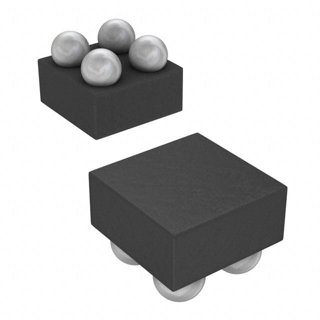
Voir les spécifications pour les détails du produit.

SN74LVC1G06YZVR
Product Overview
- Category: Integrated Circuit (IC)
- Use: Logic Gate
- Characteristics: Single Inverter Buffer/Driver
- Package: SOT-23-5
- Essence: Low-Voltage CMOS Logic
- Packaging/Quantity: Tape and Reel, 3000 pieces per reel
Specifications
- Supply Voltage Range: 1.65V to 5.5V
- Input Voltage Range: 0V to VCC
- Output Voltage Range: 0V to VCC
- Maximum Operating Frequency: 100 MHz
- Propagation Delay Time: 3.8 ns (typical)
- High-Level Output Current: -32 mA
- Low-Level Output Current: 32 mA
- Operating Temperature Range: -40°C to +85°C
Detailed Pin Configuration
The SN74LVC1G06YZVR has a total of five pins:
- GND (Ground): Connected to the ground reference potential.
- IN (Input): Receives the input signal to be inverted.
- OUT (Output): Provides the inverted output signal.
- VCC (Supply Voltage): Connected to the positive supply voltage.
- NC (No Connect): This pin is not connected internally and can be left unconnected.
Functional Features
- Single inverter buffer/driver with open-drain output.
- Compatible with both TTL and CMOS logic levels.
- Supports bidirectional data flow.
- Provides high noise immunity due to hysteresis.
- Low power consumption.
- Schmitt-trigger input allows for slow input transition without oscillation.
Advantages and Disadvantages
Advantages: - Small package size enables space-saving designs. - Wide operating voltage range allows compatibility with various systems. - Low power consumption makes it suitable for battery-powered applications. - High noise immunity ensures reliable operation in noisy environments.
Disadvantages: - Limited output current capacity compared to some other ICs. - Single inverter functionality may not be suitable for complex logic operations.
Working Principles
The SN74LVC1G06YZVR is a single inverter buffer/driver that operates on low-voltage CMOS logic. It takes an input signal and provides the inverted output signal. The open-drain output allows bidirectional data flow, making it suitable for applications such as level shifting and interfacing between different logic families. The Schmitt-trigger input ensures stable operation even with slow input transitions.
Detailed Application Field Plans
The SN74LVC1G06YZVR can be used in various applications, including but not limited to:
- Level Shifting: It can be used to convert logic levels between different voltage domains.
- Signal Inversion: It can invert the polarity of digital signals.
- Bus Buffering: It can act as a buffer to isolate multiple devices connected to a common bus.
- Clock Generation: It can generate inverted clock signals for synchronization purposes.
- Sensor Interfaces: It can interface with sensors that require level shifting or signal inversion.
Detailed and Complete Alternative Models
- SN74LVC1G04DBVR: Single Inverter Gate, SOT-23-5 package.
- SN74LVC1G07DCKR: Single Buffer/Driver with Open-Drain Output, SC-70-5 package.
- SN74LVC1G08DCKR: Single 2-Input AND Gate, SC-70-5 package.
- SN74LVC1G14DBVR: Single Schmitt-Trigger Inverter, SOT-23-5 package.
- SN74LVC1G17DCKR: Single Schmitt-Trigger Buffer/Driver, SC-70-5 package.
These alternative models offer similar functionality and characteristics to the SN74LVC1G06YZVR, providing options for different package sizes and pin configurations.
Word count: 408 words
Énumérez 10 questions et réponses courantes liées à l'application de SN74LVC1G06YZVR dans les solutions techniques
Sure! Here are 10 common questions and answers related to the application of SN74LVC1G06YZVR in technical solutions:
Q1: What is SN74LVC1G06YZVR? A1: SN74LVC1G06YZVR is a single inverter gate IC (Integrated Circuit) that is commonly used in digital logic circuits.
Q2: What is the voltage range supported by SN74LVC1G06YZVR? A2: SN74LVC1G06YZVR supports a voltage range from 1.65V to 5.5V.
Q3: What is the maximum output current of SN74LVC1G06YZVR? A3: The maximum output current of SN74LVC1G06YZVR is typically around 32mA.
Q4: Can SN74LVC1G06YZVR be used as a level shifter? A4: Yes, SN74LVC1G06YZVR can be used as a level shifter to convert signals between different voltage levels.
Q5: What is the propagation delay of SN74LVC1G06YZVR? A5: The propagation delay of SN74LVC1G06YZVR is typically around 3.8ns.
Q6: Is SN74LVC1G06YZVR suitable for high-speed applications? A6: Yes, SN74LVC1G06YZVR is designed for high-speed operation and can be used in various high-speed applications.
Q7: Can SN74LVC1G06YZVR be used in battery-powered devices? A7: Yes, SN74LVC1G06YZVR operates at low power and can be used in battery-powered devices.
Q8: Does SN74LVC1G06YZVR have built-in protection features? A8: Yes, SN74LVC1G06YZVR has built-in ESD (Electrostatic Discharge) protection to safeguard against electrostatic damage.
Q9: Can SN74LVC1G06YZVR be used in both digital and analog circuits? A9: SN74LVC1G06YZVR is primarily designed for digital logic applications, but it can also be used in certain analog circuits.
Q10: What is the package type of SN74LVC1G06YZVR? A10: SN74LVC1G06YZVR is available in a small SOT-23-5 package, which is commonly used for surface mount applications.
Please note that these answers are general and may vary depending on specific datasheet specifications and application requirements.

