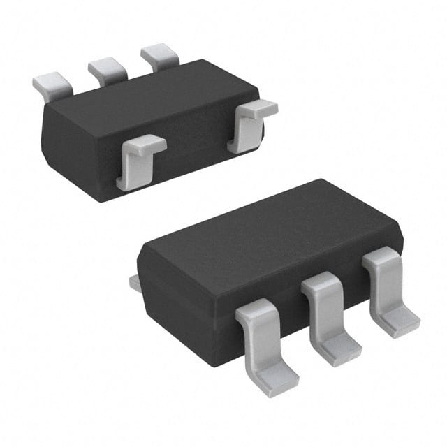
Voir les spécifications pour les détails du produit.

SN74LV1T126DCKR
Product Overview
- Category: Integrated Circuit (IC)
- Use: Logic Level Shifter
- Characteristics: Single-Bit Bus Buffer Gate with 3-State Outputs
- Package: SC-70 (6-Pin)
- Essence: This IC is designed to provide voltage level shifting for digital signals in various applications.
- Packaging/Quantity: Tape and Reel, 3000 units per reel
Specifications
- Supply Voltage Range: 1.65V to 5.5V
- High-Level Input Voltage: 2.3V to VCC
- Low-Level Input Voltage: GND to 0.8V
- High-Level Output Voltage: 2.4V (minimum) at IOH = -4mA
- Low-Level Output Voltage: 0.4V (maximum) at IOL = 4mA
- Maximum Operating Frequency: 100 MHz
Detailed Pin Configuration
The SN74LV1T126DCKR has a total of 6 pins:
- Pin 1: Input (A)
- Pin 2: Output Enable (OE)
- Pin 3: Ground (GND)
- Pin 4: Output (Y)
- Pin 5: Power Supply (VCC)
- Pin 6: Input (B)
Functional Features
- Single-bit buffer gate with 3-state outputs
- Provides voltage level shifting between different logic levels
- Allows bidirectional data flow
- Enables or disables the output using the Output Enable (OE) pin
Advantages and Disadvantages
Advantages: - Compact SC-70 package allows for space-saving designs - Wide supply voltage range enables compatibility with various systems - High-speed operation supports fast data transmission - 3-state outputs provide flexibility in bus sharing applications
Disadvantages: - Limited to single-bit data transmission - Not suitable for high-current applications
Working Principles
The SN74LV1T126DCKR is a logic level shifter that operates by receiving a digital input signal and shifting its voltage level to match the desired output level. The IC utilizes a buffer gate to amplify and condition the input signal, allowing it to be safely transmitted to the output pin. The Output Enable (OE) pin controls whether the output is enabled or disabled, providing additional control over the data flow.
Detailed Application Field Plans
The SN74LV1T126DCKR can be used in various applications, including:
- Battery-powered devices: Due to its low power consumption and wide supply voltage range, this IC is suitable for portable electronics such as smartphones, tablets, and wearables.
- Industrial automation: The logic level shifting capability makes it useful in industrial control systems, where different voltage levels are commonly encountered.
- Communication systems: This IC can be employed in communication equipment, such as routers and switches, to interface between different logic families or voltage domains.
- Automotive electronics: With its compact package and ability to handle automotive voltage levels, the SN74LV1T126DCKR finds application in automotive electronics, including infotainment systems and engine control units.
Detailed and Complete Alternative Models
- SN74LVC1T45DBVR: Single-Bit Dual Supply Bus Transceiver with Configurable Voltage Translation and 3-State Outputs
- SN74LVC1G07DCKR: Single-Bit Buffer/Driver with Open-Drain Output
- SN74LVC1G125DBVR: Single-Bit Bus Buffer Gate with 3-State Outputs and Schmitt-Trigger Inputs
These alternative models offer similar functionality and can be considered as alternatives to the SN74LV1T126DCKR.
Word count: 430 words
Énumérez 10 questions et réponses courantes liées à l'application de SN74LV1T126DCKR dans les solutions techniques
Sure! Here are 10 common questions and answers related to the application of SN74LV1T126DCKR:
Q1: What is SN74LV1T126DCKR? A1: SN74LV1T126DCKR is a single bus buffer gate with 3-state output, designed for voltage level translation.
Q2: What is the operating voltage range of SN74LV1T126DCKR? A2: The operating voltage range is from 1.65V to 5.5V.
Q3: What is the maximum output current of SN74LV1T126DCKR? A3: The maximum output current is ±32mA.
Q4: Can SN74LV1T126DCKR be used for bidirectional level translation? A4: No, SN74LV1T126DCKR is unidirectional and can only translate signals in one direction.
Q5: What is the typical propagation delay of SN74LV1T126DCKR? A5: The typical propagation delay is around 4.8ns.
Q6: Can SN74LV1T126DCKR be used in high-speed applications? A6: Yes, SN74LV1T126DCKR is suitable for high-speed applications due to its fast propagation delay.
Q7: Does SN74LV1T126DCKR have built-in ESD protection? A7: Yes, SN74LV1T126DCKR has built-in ESD protection up to 2kV.
Q8: Can SN74LV1T126DCKR drive capacitive loads? A8: Yes, SN74LV1T126DCKR can drive capacitive loads up to 50pF.
Q9: What is the package type of SN74LV1T126DCKR? A9: SN74LV1T126DCKR comes in a small SOT-353 package.
Q10: Can SN74LV1T126DCKR be used in battery-powered applications? A10: Yes, SN74LV1T126DCKR can operate at low voltages and is suitable for battery-powered applications.
Please note that these answers are general and may vary depending on specific application requirements.

