

Voir les spécifications pour les détails du produit.
SN74LV138ATDGVR
Product Overview
- Category: Integrated Circuit (IC)
- Use: Decoder/Demultiplexer
- Characteristics:
- Low-voltage operation
- High-speed performance
- Wide operating temperature range
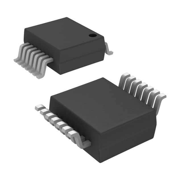
- Package: TSSOP-16
- Essence: Decodes a 3-bit binary input to one of eight outputs
- Packaging/Quantity: Tape and reel, 2500 units per reel
Specifications
- Supply Voltage Range: 1.65V to 5.5V
- Input Voltage Range: 0V to VCC
- Output Voltage Range: 0V to VCC
- Operating Temperature Range: -40°C to +125°C
- Maximum Propagation Delay: 8 ns
- Maximum Quiescent Current: 2 μA
Detailed Pin Configuration
The SN74LV138ATDGVR has a total of 16 pins, numbered as follows:
- GND (Ground)
- A0 (Input A0)
- A1 (Input A1)
- A2 (Input A2)
- Y0 (Output Y0)
- Y1 (Output Y1)
- Y2 (Output Y2)
- Y3 (Output Y3)
- Y4 (Output Y4)
- Y5 (Output Y5)
- Y6 (Output Y6)
- Y7 (Output Y7)
- E1 (Enable Input 1)
- E2 (Enable Input 2)
- VCC (Supply Voltage)
- GND (Ground)
Functional Features
- Decodes a 3-bit binary input to one of eight outputs
- Enables cascading for larger decoding applications
- Low power consumption
- Schmitt-trigger inputs for noise immunity
- Supports both CMOS and TTL voltage levels
Advantages and Disadvantages
Advantages: - Wide operating voltage range allows compatibility with various systems - High-speed performance enables efficient decoding operations - Low power consumption makes it suitable for battery-powered devices - Schmitt-trigger inputs provide robustness against noise
Disadvantages: - Limited to 3-bit binary input decoding, not suitable for larger applications - TSSOP package may require careful handling during assembly
Working Principles
The SN74LV138ATDGVR is a decoder/demultiplexer IC that takes a 3-bit binary input and activates one of the eight outputs based on the input combination. The enable inputs (E1 and E2) control the operation of the decoder. When both enable inputs are high, all outputs are disabled. By manipulating the enable inputs and providing the appropriate binary input, the desired output can be selected.
Detailed Application Field Plans
The SN74LV138ATDGVR finds applications in various fields, including:
- Address decoding in microcontrollers and microprocessors
- Memory selection in digital systems
- Data routing in communication systems
- Signal demultiplexing in multimedia devices
- Control logic in industrial automation
Detailed and Complete Alternative Models
- 74HC138: Similar functionality, but operates at higher voltage levels (2V to 6V)
- CD74HCT138: Compatible with TTL voltage levels, wider temperature range (-55°C to +125°C)
- SN54LS138: Operates at higher speeds, but requires higher supply voltage (4.75V to 5.25V)
These alternative models offer similar decoding capabilities with slight variations in voltage range, speed, and temperature tolerance.
Word count: 410 words
Énumérez 10 questions et réponses courantes liées à l'application de SN74LV138ATDGVR dans les solutions techniques
Sure! Here are 10 common questions and answers related to the application of SN74LV138ATDGVR:
Question: What is the SN74LV138ATDGVR?
Answer: The SN74LV138ATDGVR is a 3-to-8 line decoder/demultiplexer IC (integrated circuit) manufactured by Texas Instruments.Question: What is the purpose of the SN74LV138ATDGVR?
Answer: The purpose of this IC is to decode binary information from a 3-bit input and activate one of the eight output lines based on the input combination.Question: What is the voltage supply range for the SN74LV138ATDGVR?
Answer: The voltage supply range for this IC is typically between 2V and 5.5V.Question: What is the maximum output current of the SN74LV138ATDGVR?
Answer: The maximum output current per output pin is 24mA.Question: Can the SN74LV138ATDGVR be used in both digital and analog applications?
Answer: No, the SN74LV138ATDGVR is specifically designed for digital applications and should not be used in analog circuits.Question: How can I select the desired output line using the SN74LV138ATDGVR?
Answer: The desired output line can be selected by providing the appropriate binary input combination to the three input pins (A0, A1, and A2).Question: What is the propagation delay of the SN74LV138ATDGVR?
Answer: The propagation delay is the time it takes for the output to respond to a change in the input signal. For the SN74LV138ATDGVR, the typical propagation delay is around 9ns.Question: Can the SN74LV138ATDGVR be cascaded to increase the number of output lines?
Answer: Yes, multiple SN74LV138ATDGVR ICs can be cascaded together to increase the number of output lines by connecting the enable (E1, E2, and E3) pins in parallel.Question: What is the package type for the SN74LV138ATDGVR?
Answer: The SN74LV138ATDGVR comes in a small SOT-23-16 package.Question: Are there any specific precautions to consider when using the SN74LV138ATDGVR?
Answer: It is important to ensure that the voltage supply does not exceed the specified range, and proper decoupling capacitors should be used to minimize noise and stabilize the power supply. Additionally, care should be taken to avoid exceeding the maximum output current per pin.