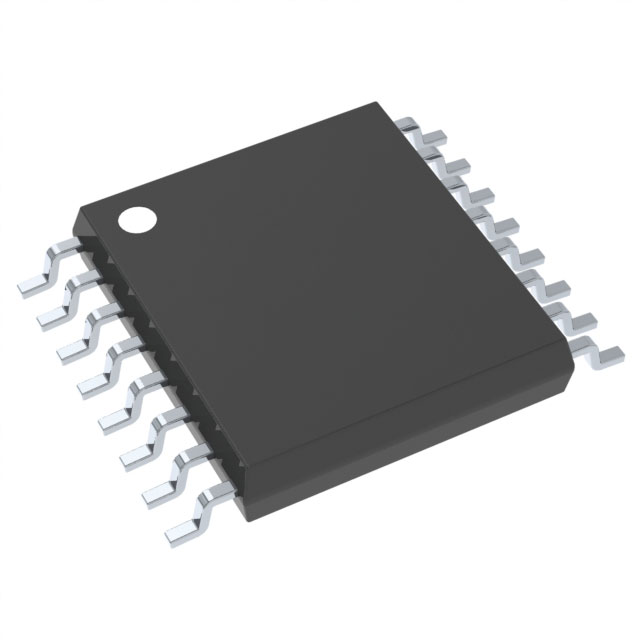
Voir les spécifications pour les détails du produit.

SN74HC138QPWRG4Q1
Product Overview
Category
SN74HC138QPWRG4Q1 belongs to the category of integrated circuits (ICs).
Use
This product is commonly used in electronic devices for decoding and demultiplexing applications.
Characteristics
- High-speed CMOS technology
- Low power consumption
- Wide operating voltage range
- Schmitt-trigger inputs for noise immunity
- 3-to-8 line decoder/demultiplexer functionality
Package
SN74HC138QPWRG4Q1 is available in a small-sized TSSOP-16 package.
Essence
The essence of this product lies in its ability to decode and demultiplex multiple input signals into separate output lines, enabling efficient data routing and control in electronic systems.
Packaging/Quantity
SN74HC138QPWRG4Q1 is typically packaged in reels containing 2500 units.
Specifications
- Supply Voltage: 2V to 6V
- Input Voltage: 0V to VCC
- Output Voltage: 0V to VCC
- Operating Temperature Range: -40°C to +125°C
- Propagation Delay Time: 13 ns (typical)
- Output Current: ±25 mA
Detailed Pin Configuration
The pin configuration of SN74HC138QPWRG4Q1 is as follows:
+---+--+---+
   A2 --|1  +--+ 16|-- VCC
   A1 --|2       15|-- Y7
   A0 --|3       14|-- Y6
  /E1 --|4       13|-- Y5
  /E2 --|5       12|-- Y4
  /E3 --|6       11|-- Y3
   Y0 --|7       10|-- Y2
   Y1 --|8        9|-- GND
        +----------+
Functional Features
- Decodes three binary address inputs (A0, A1, A2) into eight mutually exclusive outputs (Y0-Y7).
- Enables the selection of one output line at a time based on the input address.
- Supports active-low enable inputs (/E1, /E2, /E3) for easy control of the decoder functionality.
Advantages and Disadvantages
Advantages
- High-speed operation allows for efficient data processing.
- Low power consumption makes it suitable for battery-powered devices.
- Wide operating voltage range provides flexibility in various applications.
- Schmitt-trigger inputs ensure noise immunity, enhancing signal integrity.
Disadvantages
- Limited to 3-to-8 line decoding/demultiplexing functionality.
- May require additional components for complex addressing schemes.
Working Principles
SN74HC138QPWRG4Q1 operates by receiving three binary address inputs (A0, A1, A2) and generating eight output lines (Y0-Y7). The selected output line is determined by the input address. The active-low enable inputs (/E1, /E2, /E3) control the decoder's functionality, allowing for easy activation or deactivation of the decoding process.
Detailed Application Field Plans
SN74HC138QPWRG4Q1 finds applications in various fields, including: 1. Digital multiplexing systems 2. Address decoding in microcontrollers 3. Memory selection in computer systems 4. Data routing in communication devices 5. Control circuitry in industrial automation
Detailed and Complete Alternative Models
Some alternative models that offer similar functionality to SN74HC138QPWRG4Q1 include: 1. CD74HC138E - CMOS 3-to-8 line decoder/demultiplexer 2. 74HC138N - High-speed CMOS logic decoder/demultiplexer 3. SN54HC138J - Schottky-clamped high-performance CMOS decoder/demultiplexer
These alternative models can be considered based on specific requirements and availability.
Word count: 489 words
Énumérez 10 questions et réponses courantes liées à l'application de SN74HC138QPWRG4Q1 dans les solutions techniques
Sure! Here are 10 common questions and answers related to the application of SN74HC138QPWRG4Q1 in technical solutions:
1. What is SN74HC138QPWRG4Q1? - SN74HC138QPWRG4Q1 is a high-speed CMOS 3-to-8 line decoder/demultiplexer IC, which can be used in various digital applications.
2. What is the operating voltage range of SN74HC138QPWRG4Q1? - The operating voltage range of SN74HC138QPWRG4Q1 is from 2V to 6V.
3. What is the maximum output current of SN74HC138QPWRG4Q1? - The maximum output current of SN74HC138QPWRG4Q1 is 25mA.
4. Can SN74HC138QPWRG4Q1 be used as a demultiplexer? - Yes, SN74HC138QPWRG4Q1 can be used as a demultiplexer to decode a binary address into one of eight outputs.
5. How many input lines does SN74HC138QPWRG4Q1 have? - SN74HC138QPWRG4Q1 has three input lines (A0, A1, and A2) for addressing the desired output.
6. What is the propagation delay of SN74HC138QPWRG4Q1? - The propagation delay of SN74HC138QPWRG4Q1 is typically around 13 ns.
7. Can SN74HC138QPWRG4Q1 be cascaded to increase the number of outputs? - Yes, multiple SN74HC138QPWRG4Q1 ICs can be cascaded together to increase the number of outputs.
8. What is the power supply current of SN74HC138QPWRG4Q1? - The power supply current of SN74HC138QPWRG4Q1 is typically around 2 mA.
9. Is SN74HC138QPWRG4Q1 compatible with TTL logic levels? - Yes, SN74HC138QPWRG4Q1 is compatible with both CMOS and TTL logic levels.
10. Can SN74HC138QPWRG4Q1 be used in automotive applications? - Yes, SN74HC138QPWRG4Q1 is specifically designed for automotive applications and is qualified to meet automotive standards.
Please note that these answers are general and may vary depending on the specific datasheet and application requirements.

