

Voir les spécifications pour les détails du produit.
SN74ALVC16835DGVR
Product Overview
- Category: Integrated Circuit
- Use: Logic Level Translator
- Characteristics: High-speed, low-power, voltage level shifting
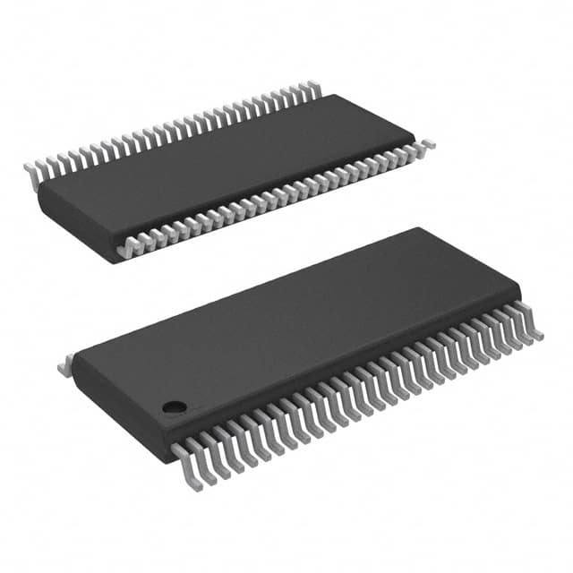
- Package: VSSOP (Very Small Outline Package)
- Essence: Logic level translation between different voltage domains
- Packaging/Quantity: Tape and Reel, 2500 units per reel
Specifications
- Supply Voltage Range: 1.65V to 3.6V
- Input Voltage Range: 0V to VCC
- Output Voltage Range: 0V to VCC
- Operating Temperature Range: -40°C to +85°C
- Propagation Delay: 2.5ns (typical)
- Maximum Frequency: 400MHz
Detailed Pin Configuration
The SN74ALVC16835DGVR has a total of 48 pins, which are divided into four groups:
- Group A (pins 1-12): Inputs from voltage domain A
- Group B (pins 13-24): Outputs to voltage domain B
- Group C (pins 25-36): Inputs from voltage domain B
- Group D (pins 37-48): Outputs to voltage domain A
Each pin serves a specific purpose in the logic level translation process.
Functional Features
- Bidirectional voltage level translation between two voltage domains
- Automatic direction control based on input signal levels
- High-speed operation with minimal propagation delay
- Low power consumption for energy-efficient applications
- ESD protection for enhanced reliability
- Wide operating temperature range for versatile usage
Advantages and Disadvantages
Advantages: - Enables seamless communication between devices operating at different voltage levels - Fast data transmission with minimal delay - Low power consumption extends battery life in portable devices - Robust ESD protection ensures reliable operation
Disadvantages: - Limited to voltage translation between specific voltage domains - Requires careful consideration of input and output voltage levels to prevent damage
Working Principles
The SN74ALVC16835DGVR utilizes a combination of CMOS technology and level-shifting circuitry to achieve voltage translation. It automatically detects the input signal levels and adjusts the direction of data flow accordingly. The integrated circuit ensures minimal propagation delay, allowing for high-speed data transmission between different voltage domains.
Detailed Application Field Plans
The SN74ALVC16835DGVR is commonly used in various applications that require voltage level translation, such as:
- Microcontroller interfacing with different voltage peripherals
- Communication interfaces between devices operating at different voltage levels
- Battery-powered systems where power efficiency is crucial
- Industrial automation systems with mixed voltage components
- Consumer electronics for seamless integration of diverse devices
Detailed and Complete Alternative Models
- SN74LVC1T45DBVR: Single-bit dual-supply level translator
- SN74AVC4T245RGYR: Quad-bit level shifter with 3-state outputs
- SN74AHCT125DR: Quad-buffer gate with voltage level translation
- SN74LVCH16244ADGGR: 16-bit bus transceiver with voltage level shifting
- SN74CBTLV3257PWR: Quad multiplexer/demultiplexer with voltage translation
These alternative models offer similar functionality and can be considered based on specific application requirements.
Word count: 315 words
Énumérez 10 questions et réponses courantes liées à l'application de SN74ALVC16835DGVR dans les solutions techniques
Sure! Here are 10 common questions and answers related to the application of SN74ALVC16835DGVR:
Q: What is SN74ALVC16835DGVR? A: SN74ALVC16835DGVR is a 18-bit universal bus driver with 3-state outputs, commonly used in digital systems.
Q: What is the operating voltage range for SN74ALVC16835DGVR? A: The operating voltage range for SN74ALVC16835DGVR is typically between 1.65V and 3.6V.
Q: Can SN74ALVC16835DGVR be used as a level shifter? A: Yes, SN74ALVC16835DGVR can be used as a level shifter to convert signals between different voltage levels.
Q: How many output pins does SN74ALVC16835DGVR have? A: SN74ALVC16835DGVR has 18 output pins, each capable of driving up to 24mA.
Q: What is the maximum data rate supported by SN74ALVC16835DGVR? A: SN74ALVC16835DGVR supports a maximum data rate of 400Mbps.
Q: Can SN74ALVC16835DGVR be used in high-speed applications? A: Yes, SN74ALVC16835DGVR is suitable for high-speed applications due to its fast propagation delay and minimal skew.
Q: Does SN74ALVC16835DGVR have built-in ESD protection? A: Yes, SN74ALVC16835DGVR features built-in ESD protection on all inputs and outputs.
Q: Can SN74ALVC16835DGVR be used in automotive applications? A: Yes, SN74ALVC16835DGVR is qualified for automotive applications and meets the necessary standards.
Q: What is the power supply current consumption of SN74ALVC16835DGVR? A: The power supply current consumption of SN74ALVC16835DGVR varies depending on the operating conditions but typically ranges from 2mA to 20mA.
Q: Can SN74ALVC16835DGVR be used in multi-voltage systems? A: Yes, SN74ALVC16835DGVR can be used in multi-voltage systems as it supports mixed voltage operation.
Please note that these answers are general and may vary based on specific application requirements. It's always recommended to refer to the datasheet and consult with technical experts for accurate information.