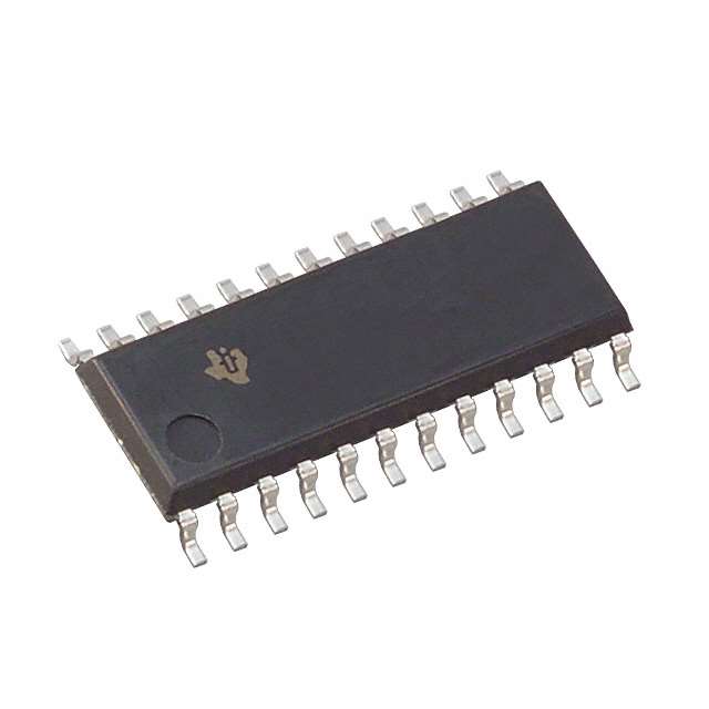
Voir les spécifications pour les détails du produit.

SN74ABT657ANSRE4
Product Overview
- Category: Integrated Circuit
- Use: Data Bus Transceiver
- Characteristics: High-speed, Bi-directional, 8-bit, Non-inverting
- Package: SOIC (Small Outline Integrated Circuit)
- Essence: Transfers data between two bidirectional buses
- Packaging/Quantity: Tape and Reel, 2500 units per reel
Specifications
- Supply Voltage Range: 4.5V to 5.5V
- Input Voltage Range: 0V to VCC
- Output Voltage Range: 0V to VCC
- Operating Temperature Range: -40°C to +85°C
- Maximum Propagation Delay: 6ns
- Maximum Operating Frequency: 100MHz
Pin Configuration
The SN74ABT657ANSRE4 has a total of 24 pins. The pin configuration is as follows:
- OE (Output Enable) A
- A1 (Data Bus A Bit 1)
- A2 (Data Bus A Bit 2)
- A3 (Data Bus A Bit 3)
- A4 (Data Bus A Bit 4)
- A5 (Data Bus A Bit 5)
- A6 (Data Bus A Bit 6)
- A7 (Data Bus A Bit 7)
- A8 (Data Bus A Bit 8)
- GND (Ground)
- B8 (Data Bus B Bit 8)
- B7 (Data Bus B Bit 7)
- B6 (Data Bus B Bit 6)
- B5 (Data Bus B Bit 5)
- B4 (Data Bus B Bit 4)
- B3 (Data Bus B Bit 3)
- B2 (Data Bus B Bit 2)
- B1 (Data Bus B Bit 1)
- OE (Output Enable) B
- VCC (Supply Voltage)
- DIR (Direction Control)
- GND (Ground)
- NC (No Connection)
- NC (No Connection)
Functional Features
- Bi-directional data transfer between two buses
- Non-inverting logic
- High-speed operation
- Output enable control for each bus
- Direction control for selecting the data flow
Advantages and Disadvantages
Advantages: - High-speed operation allows for efficient data transfer - Bi-directional functionality simplifies circuit design - Non-inverting logic ensures accurate data transmission
Disadvantages: - Limited to 8-bit data bus width - Requires careful consideration of direction control to avoid data conflicts
Working Principles
The SN74ABT657ANSRE4 is a bidirectional data bus transceiver that enables data transfer between two buses. It operates by using an output enable signal and a direction control signal to determine the data flow. When the output enable signal is active, the transceiver allows data to be transferred in both directions. The direction control signal determines whether the data flows from Bus A to Bus B or vice versa.
Detailed Application Field Plans
The SN74ABT657ANSRE4 can be used in various applications where bidirectional data transfer is required. Some potential application fields include:
- Microprocessor Systems: Facilitating communication between the microprocessor and external devices.
- Data Communication Networks: Enabling data exchange between different network components.
- Industrial Automation: Transferring data between control systems and peripheral devices.
- Automotive Electronics: Connecting various electronic modules within a vehicle.
- Test and Measurement Equipment: Providing data transfer capabilities in testing setups.
Detailed and Complete Alternative Models
- SN74ABT657ADW: Wide SOIC package, 24 pins
- SN74ABT657ADB: SSOP (Shrink Small Outline Package) package, 24 pins
- SN74ABT657APW: TSSOP (Thin Shrink Small Outline Package) package, 24 pins
- SN74ABT657ANSR: SOIC package, 24 pins
These alternative models offer similar functionality and characteristics to the SN74ABT657ANSRE4, providing flexibility in choosing the most suitable option for specific applications.
Word count: 346 words
Énumérez 10 questions et réponses courantes liées à l'application de SN74ABT657ANSRE4 dans les solutions techniques
Sure! Here are 10 common questions and answers related to the application of SN74ABT657ANSRE4 in technical solutions:
Q: What is the SN74ABT657ANSRE4? A: The SN74ABT657ANSRE4 is a 16-bit bus transceiver with parity, designed for high-speed digital systems.
Q: What is the maximum operating frequency of the SN74ABT657ANSRE4? A: The SN74ABT657ANSRE4 can operate at frequencies up to 100 MHz.
Q: Can the SN74ABT657ANSRE4 be used for bidirectional data transfer? A: Yes, the SN74ABT657ANSRE4 supports bidirectional data transfer on its 16-bit bus.
Q: Does the SN74ABT657ANSRE4 have built-in parity generation and checking? A: Yes, the SN74ABT657ANSRE4 has built-in parity generation and checking functionality.
Q: What is the voltage supply range for the SN74ABT657ANSRE4? A: The SN74ABT657ANSRE4 operates with a voltage supply range of 4.5V to 5.5V.
Q: Can the SN74ABT657ANSRE4 handle level translation between different voltage domains? A: Yes, the SN74ABT657ANSRE4 can perform level translation between different voltage domains.
Q: What is the output drive strength of the SN74ABT657ANSRE4? A: The SN74ABT657ANSRE4 has a typical output drive strength of ±12mA.
Q: Is the SN74ABT657ANSRE4 compatible with TTL and CMOS logic levels? A: Yes, the SN74ABT657ANSRE4 is compatible with both TTL and CMOS logic levels.
Q: Can the SN74ABT657ANSRE4 be used in hot-swappable applications? A: No, the SN74ABT657ANSRE4 is not designed for hot-swappable applications.
Q: What package options are available for the SN74ABT657ANSRE4? A: The SN74ABT657ANSRE4 is available in a 56-pin SSOP package.
Please note that these answers are general and may vary depending on the specific application and requirements.

