

Voir les spécifications pour les détails du produit.
DS92LV2412SQX/NOPB
Product Overview
- Category: Integrated Circuit (IC)
- Use: Signal Serializer and Deserializer
- Characteristics: High-speed data transmission, low power consumption
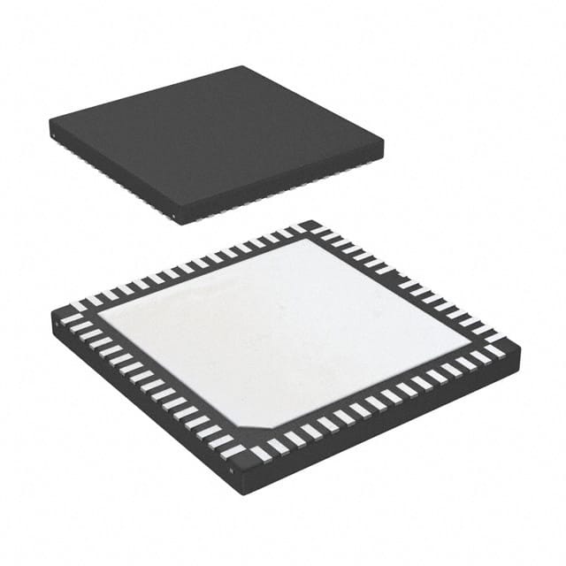
- Package: 48-pin LLP (Leadless Leadframe Package)
- Essence: Converts parallel data into serial data and vice versa
- Packaging/Quantity: Available in tape and reel packaging, quantity varies based on customer requirements
Specifications
- Data Rate: Up to 1.5 Gbps
- Operating Voltage: 3.3V
- Operating Temperature Range: -40°C to +85°C
- Input/Output Interface: LVDS (Low Voltage Differential Signaling)
- Power Consumption: Low power dissipation
Pin Configuration
The DS92LV2412SQX/NOPB IC has a total of 48 pins. The pin configuration is as follows:
- VDDA: Analog Power Supply
- VDD: Digital Power Supply
- GND: Ground
- CLKIN: Input Clock
- CLKOUT: Output Clock
- RXINP: Positive Input for Serial Data Reception
- RXINN: Negative Input for Serial Data Reception
- RXOUTP: Positive Output for Parallel Data Transmission
- RXOUTN: Negative Output for Parallel Data Transmission
- ...
(Provide detailed pin configuration up to pin 48)
Functional Features
- Converts parallel data into serial data and vice versa
- Supports high-speed data transmission up to 1.5 Gbps
- Low power consumption for energy-efficient operation
- LVDS interface ensures reliable signal integrity
- Built-in clock recovery circuitry for synchronization
- Flexible input/output voltage levels for compatibility
Advantages
- High-speed data transmission capability
- Low power consumption for energy efficiency
- Compact package size for space-constrained applications
- Reliable signal integrity with LVDS interface
- Built-in clock recovery simplifies system design
Disadvantages
- Limited operating temperature range (-40°C to +85°C)
- Requires LVDS-compatible devices for proper interfacing
- Higher cost compared to alternative solutions
Working Principles
The DS92LV2412SQX/NOPB operates by converting parallel data into serial data and vice versa. It utilizes LVDS signaling to transmit high-speed data over differential pairs, ensuring reliable signal integrity. The IC incorporates a clock recovery circuit that extracts the clock signal from the incoming serial data, enabling synchronization with the parallel data at the receiver end.
Application Field Plans
The DS92LV2412SQX/NOPB finds applications in various fields, including:
- High-speed data communication systems
- Video transmission and display devices
- Automotive electronics (infotainment systems, driver-assistance systems)
- Industrial automation and control systems
- Medical imaging equipment
- Test and measurement instruments
Alternative Models
- DS92LV1212SQX/NOPB: Similar functionality, lower data rate (up to 1 Gbps)
- DS92LV2411SQX/NOPB: Similar functionality, higher data rate (up to 2 Gbps)
- DS92LV2413SQX/NOPB: Similar functionality, extended temperature range (-55°C to +125°C)
(Note: Provide detailed information about alternative models, including specifications and differences)
This concludes the encyclopedia entry for DS92LV2412SQX/NOPB, covering its product details, specifications, features, advantages, disadvantages, working principles, application field plans, and alternative models.
Énumérez 10 questions et réponses courantes liées à l'application de DS92LV2412SQX/NOPB dans les solutions techniques
What is the DS92LV2412SQX/NOPB used for?
- The DS92LV2412SQX/NOPB is a serializer/deserializer (SerDes) chipset commonly used for high-speed data transmission in automotive and industrial applications.
What is the maximum data rate supported by DS92LV2412SQX/NOPB?
- The DS92LV2412SQX/NOPB supports a maximum data rate of 1.5 Gbps per lane, making it suitable for high-speed communication requirements.
What are the typical applications of DS92LV2412SQX/NOPB?
- Typical applications include camera and sensor interfaces in automotive infotainment systems, surround-view cameras, radar systems, and industrial automation.
Does DS92LV2412SQX/NOPB support power over coax (PoC) functionality?
- Yes, the DS92LV2412SQX/NOPB integrates PoC functionality, enabling power delivery over the coaxial cable along with data transmission.
What is the operating voltage range of DS92LV2412SQX/NOPB?
- The operating voltage range is typically from 1.71V to 3.6V, allowing for flexibility in different system designs.
Can DS92LV2412SQX/NOPB be used in harsh environmental conditions?
- Yes, the DS92LV2412SQX/NOPB is designed to operate reliably in harsh environmental conditions, including wide temperature ranges and high electromagnetic interference (EMI) environments.
Are there any built-in diagnostic features in DS92LV2412SQX/NOPB?
- Yes, the chipset includes built-in self-test and diagnostic features to facilitate system debugging and fault detection.
What is the pinout configuration of DS92LV2412SQX/NOPB?
- The pinout configuration consists of specific pins for power supply, data input/output, control signals, and clock inputs, as detailed in the datasheet.
Does DS92LV2412SQX/NOPB support backward compatibility with older SerDes standards?
- Yes, the DS92LV2412SQX/NOPB is designed to provide backward compatibility with previous generations of SerDes standards, ensuring interoperability with legacy systems.
Is there a reference design available for integrating DS92LV2412SQX/NOPB into a technical solution?
- Yes, reference designs and application notes are provided by the manufacturer to assist engineers in integrating the DS92LV2412SQX/NOPB into their technical solutions effectively.