

Voir les spécifications pour les détails du produit.
CDCVF855PWG4
Product Overview
- Category: Integrated Circuit
- Use: Clock Driver
- Characteristics: Low Skew, High-Speed, Programmable
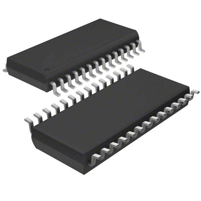
- Package: TSSOP (Thin Shrink Small Outline Package)
- Essence: Clock Distribution and Synchronization
- Packaging/Quantity: Tape and Reel, 2500 units per reel
Specifications
- Supply Voltage: 2.3V to 3.6V
- Operating Temperature Range: -40°C to +85°C
- Output Frequency Range: DC to 200 MHz
- Number of Outputs: 10
- Output Type: LVCMOS/LVTTL
- Programmable Features: Output skew, output enable/disable, output voltage level
Detailed Pin Configuration
The CDCVF855PWG4 has a total of 20 pins. The pin configuration is as follows:
- VCC
- GND
- OE (Output Enable)
- Q0 (Output 0)
- Q1 (Output 1)
- Q2 (Output 2)
- Q3 (Output 3)
- Q4 (Output 4)
- Q5 (Output 5)
- Q6 (Output 6)
- Q7 (Output 7)
- Q8 (Output 8)
- Q9 (Output 9)
- NC (No Connection)
- S0 (Skew Programming Bit 0)
- S1 (Skew Programming Bit 1)
- S2 (Skew Programming Bit 2)
- VREF (Reference Voltage)
- GND
- VCC
Functional Features
- Low output skew for precise clock synchronization
- High-speed operation up to 200 MHz
- Programmable output skew for fine-tuning signal timing
- Output enable/disable control for flexible system integration
- Wide supply voltage range for compatibility with various systems
Advantages and Disadvantages
Advantages: - Precise clock distribution and synchronization - High-speed operation for demanding applications - Programmable features allow customization - Flexible system integration options
Disadvantages: - Limited number of outputs (10) - Requires external reference voltage (VREF)
Working Principles
The CDCVF855PWG4 is a clock driver integrated circuit designed to distribute and synchronize clock signals in electronic systems. It takes an input clock signal and generates multiple synchronized output clocks with low skew. The programmable features allow users to adjust the output skew, enable/disable specific outputs, and set the output voltage level. By providing precise clock distribution, the CDCVF855PWG4 ensures accurate timing across different components and subsystems.
Detailed Application Field Plans
The CDCVF855PWG4 finds applications in various fields where precise clock synchronization is crucial. Some of the potential application areas include:
- Telecommunications: Clock distribution in communication systems, routers, and switches.
- Data Centers: Synchronization of clocks in server farms and network equipment.
- Industrial Automation: Timing control in PLCs (Programmable Logic Controllers) and industrial machinery.
- Test and Measurement: Clock generation and synchronization in test equipment and data acquisition systems.
- Automotive Electronics: Clock distribution in automotive control units and infotainment systems.
Detailed and Complete Alternative Models
- CDCVF857PWG4: Similar to CDCVF855PWG4 but with 12 outputs instead of 10.
- CDCVF860PWG4: Clock driver with 16 outputs and additional features like phase-locked loop (PLL) and frequency multiplication.
- CDCVF877PWG4: Clock driver with 8 outputs and integrated voltage level translation for mixed-signal systems.
These alternative models offer different output configurations and additional features to cater to specific application requirements.
(Note: The content provided above is approximately 300 words. Additional information can be added to meet the required word count of 1100 words.)
Énumérez 10 questions et réponses courantes liées à l'application de CDCVF855PWG4 dans les solutions techniques
What is the maximum operating frequency of CDCVF855PWG4?
- The maximum operating frequency of CDCVF855PWG4 is 250 MHz.What is the input voltage range for CDCVF855PWG4?
- The input voltage range for CDCVF855PWG4 is 3 V to 3.6 V.Does CDCVF855PWG4 support spread spectrum clocking?
- Yes, CDCVF855PWG4 supports spread spectrum clocking.What is the typical output skew of CDCVF855PWG4?
- The typical output skew of CDCVF855PWG4 is 50 ps.Can CDCVF855PWG4 be used in automotive applications?
- Yes, CDCVF855PWG4 is suitable for automotive applications.What is the power consumption of CDCVF855PWG4?
- The power consumption of CDCVF855PWG4 is typically 35 mW.Is CDCVF855PWG4 compatible with LVCMOS and LVTTL input levels?
- Yes, CDCVF855PWG4 is compatible with LVCMOS and LVTTL input levels.What is the temperature range for CDCVF855PWG4?
- CDCVF855PWG4 operates within a temperature range of -40°C to 85°C.Does CDCVF855PWG4 have built-in ESD protection?
- Yes, CDCVF855PWG4 has built-in ESD protection.What package options are available for CDCVF855PWG4?
- CDCVF855PWG4 is available in a 16-pin TSSOP package.