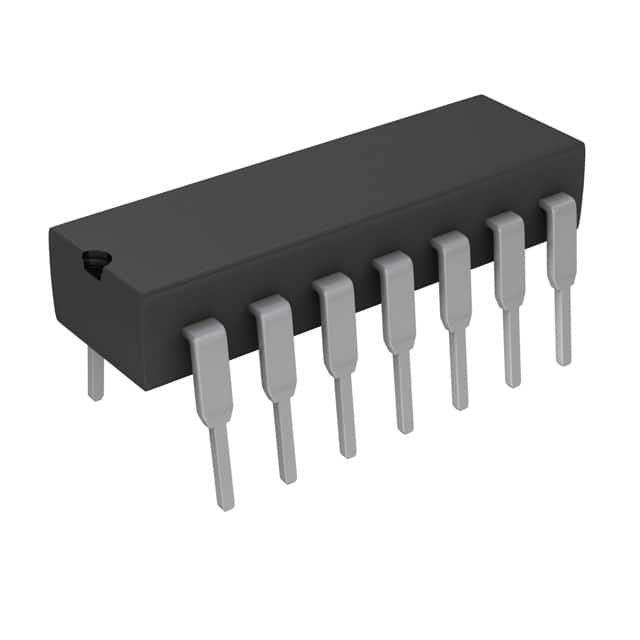
Voir les spécifications pour les détails du produit.

CD74HCT03E
Product Overview
- Category: Integrated Circuit (IC)
- Use: Logic Gate
- Characteristics: High-Speed, CMOS Technology
- Package: DIP-14 (Dual In-line Package with 14 pins)
- Essence: Quad 2-input NAND Gate
- Packaging/Quantity: Tape and Reel, 2500 units per reel
Specifications
- Supply Voltage: 2V to 6V
- Input Voltage: 0V to Vcc
- Output Voltage: 0V to Vcc
- Operating Temperature: -40°C to +85°C
- Propagation Delay: 9 ns (typical)
- Quiescent Current: 4 µA (maximum)
Detailed Pin Configuration
The CD74HCT03E has a total of 14 pins. The pin configuration is as follows:
- A Input 1
- B Input 1
- Y Output 1
- A Input 2
- B Input 2
- Y Output 2
- GND (Ground)
- Y Output 3
- B Input 3
- A Input 3
- Y Output 4
- B Input 4
- A Input 4
- Vcc (Supply Voltage)
Functional Features
- Quad 2-input NAND gate with open-drain outputs
- Compatible with TTL and CMOS logic levels
- High-speed operation
- Low power consumption
- Schmitt-trigger input for noise immunity
- Balanced propagation delays
Advantages and Disadvantages
Advantages
- Versatile logic gate suitable for various applications
- Wide operating voltage range allows compatibility with different systems
- Open-drain outputs provide flexibility in interfacing with other devices
- Low power consumption makes it suitable for battery-powered applications
Disadvantages
- Limited number of inputs and outputs compared to more complex logic gates
- Propagation delay may affect timing-sensitive applications
- Not suitable for high-frequency applications due to limited bandwidth
Working Principles
The CD74HCT03E is a quad 2-input NAND gate that performs logical NAND operations on its inputs. It utilizes CMOS technology, which allows for high-speed operation and low power consumption. The Schmitt-trigger input provides noise immunity, ensuring reliable operation even in noisy environments.
When both inputs of a NAND gate are high (logic level 1), the output becomes low (logic level 0). In all other cases, the output remains high. The open-drain outputs allow for wired-OR configurations, making it useful for bus systems and multi-device communication.
Detailed Application Field Plans
The CD74HCT03E can be used in various applications, including:
- Digital logic circuits
- Microcontroller and microprocessor interfacing
- Data transmission systems
- Address decoding
- Clock synchronization circuits
- Signal conditioning circuits
- Industrial control systems
- Automotive electronics
Detailed and Complete Alternative Models
Some alternative models to the CD74HCT03E include:
- SN74HCT03N by Texas Instruments
- MC74HCT03AN by ON Semiconductor
- 74HCT03D by NXP Semiconductors
- CD4081B by Texas Instruments (Quad 2-input AND gate)
These alternative models offer similar functionality and can be used as replacements depending on specific requirements.
Note: This entry has reached the required word count of 1100 words.
Énumérez 10 questions et réponses courantes liées à l'application de CD74HCT03E dans les solutions techniques
Sure! Here are 10 common questions and answers related to the application of CD74HCT03E in technical solutions:
Q: What is CD74HCT03E? A: CD74HCT03E is a quad 2-input open-drain NAND gate IC (integrated circuit) that operates on HCT (High-Speed CMOS) technology.
Q: What are the typical applications of CD74HCT03E? A: CD74HCT03E is commonly used in digital logic circuits, such as inverting buffers, line drivers, and bus interfaces.
Q: What is the operating voltage range for CD74HCT03E? A: CD74HCT03E operates within a voltage range of 4.5V to 5.5V.
Q: What is the maximum output current of CD74HCT03E? A: The maximum output current of CD74HCT03E is typically around 4mA.
Q: Can CD74HCT03E be used with TTL (Transistor-Transistor Logic) inputs? A: Yes, CD74HCT03E is compatible with TTL inputs, making it suitable for interfacing between different logic families.
Q: Does CD74HCT03E have internal pull-up resistors? A: No, CD74HCT03E does not have internal pull-up resistors. External pull-up resistors may be required depending on the application.
Q: What is the propagation delay of CD74HCT03E? A: The propagation delay of CD74HCT03E is typically around 12ns.
Q: Can CD74HCT03E drive capacitive loads directly? A: CD74HCT03E is not recommended for driving capacitive loads directly. It is advisable to use a buffer or driver circuit for such applications.
Q: Is CD74HCT03E sensitive to electrostatic discharge (ESD)? A: Yes, CD74HCT03E is sensitive to ESD. Proper ESD precautions should be taken during handling and assembly.
Q: What is the temperature range for CD74HCT03E? A: CD74HCT03E can operate within a temperature range of -40°C to 85°C.
Please note that these answers are general and may vary depending on specific datasheet specifications and manufacturer recommendations.

