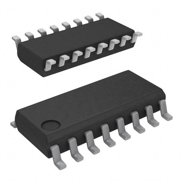
Voir les spécifications pour les détails du produit.

CD74HC237M96G4
Product Overview
- Category: Integrated Circuit
- Use: Decoding and Demultiplexing
- Characteristics: High-Speed CMOS Logic, 3-to-8 Line Decoder/Demultiplexer
- Package: SOIC-16
- Essence: Efficient decoding and demultiplexing of signals
- Packaging/Quantity: Tape and Reel, 2500 units per reel
Specifications
- Logic Family: HC
- Number of Inputs: 3
- Number of Outputs: 8
- Supply Voltage Range: 2V to 6V
- Propagation Delay: 14 ns (typical)
- Operating Temperature Range: -40°C to +85°C
Detailed Pin Configuration
- GND (Ground)
- A0 (Input A0)
- A1 (Input A1)
- A2 (Input A2)
- E1 (Enable Input 1)
- E2 (Enable Input 2)
- Y0 (Output Y0)
- Y1 (Output Y1)
- Y2 (Output Y2)
- Y3 (Output Y3)
- Y4 (Output Y4)
- Y5 (Output Y5)
- Y6 (Output Y6)
- Y7 (Output Y7)
- VCC (Positive Supply Voltage)
Functional Features
- Decodes a 3-bit binary input into one of eight outputs
- Demultiplexes the selected output based on the enable inputs
- High-speed operation suitable for time-critical applications
- Low power consumption in CMOS technology
- Wide supply voltage range allows compatibility with various systems
Advantages and Disadvantages
Advantages
- Efficient decoding and demultiplexing of signals
- High-speed operation for time-critical applications
- Low power consumption in CMOS technology
- Wide supply voltage range allows compatibility with various systems
Disadvantages
- Limited number of inputs and outputs (3-to-8 configuration)
- Propagation delay may affect timing-sensitive applications
Working Principles
The CD74HC237M96G4 is a 3-to-8 line decoder/demultiplexer integrated circuit. It takes a 3-bit binary input and decodes it into one of eight possible outputs. The selected output is determined by the combination of the input bits. The enable inputs (E1 and E2) control the demultiplexing of the selected output.
The IC operates on a wide supply voltage range of 2V to 6V, making it compatible with various systems. It utilizes high-speed CMOS logic, allowing for efficient decoding and demultiplexing of signals. The low power consumption of CMOS technology ensures energy efficiency.
However, it is important to consider the propagation delay of approximately 14 ns (typical) when using this IC in timing-sensitive applications.
Detailed Application Field Plans
The CD74HC237M96G4 can be used in various applications that require decoding and demultiplexing of signals. Some potential application fields include:
- Address Decoding: Used in microcontrollers and memory systems to decode address lines and select specific memory locations.
- Data Routing: Enables the selection of specific data paths in communication systems or multiplexers.
- Display Control: Used in LED or LCD display systems to control individual segments or pixels.
- Instrumentation: Allows for signal routing and selection in test and measurement equipment.
- Industrial Automation: Used in control systems to route signals based on specific conditions or inputs.
Detailed and Complete Alternative Models
- SN74HC138: 3-to-8 line decoder/demultiplexer from Texas Instruments.
- CD74HCT238: High-speed CMOS logic 3-to-8 line decoder/demultiplexer from Texas Instruments.
- 74HC238: 3-to-8 line decoder/demultiplexer from various manufacturers.
These alternative models offer similar functionality and can be considered as alternatives to the CD74HC237M96G4 based on specific requirements and availability.
Word count: 511 words
Énumérez 10 questions et réponses courantes liées à l'application de CD74HC237M96G4 dans les solutions techniques
Sure! Here are 10 common questions and answers related to the application of CD74HC237M96G4 in technical solutions:
Q: What is CD74HC237M96G4? A: CD74HC237M96G4 is a high-speed CMOS (Complementary Metal-Oxide-Semiconductor) 3-to-8 line decoder/demultiplexer IC.
Q: What is the purpose of CD74HC237M96G4? A: CD74HC237M96G4 is used to decode binary information from three inputs into eight outputs, making it useful for address decoding, memory selection, and other digital logic applications.
Q: What is the voltage range supported by CD74HC237M96G4? A: CD74HC237M96G4 supports a voltage range of 2V to 6V.
Q: What is the maximum operating frequency of CD74HC237M96G4? A: The maximum operating frequency of CD74HC237M96G4 is typically around 74 MHz.
Q: Can CD74HC237M96G4 be used with both TTL and CMOS logic levels? A: Yes, CD74HC237M96G4 is compatible with both TTL and CMOS logic levels, making it versatile for various applications.
Q: How many enable inputs does CD74HC237M96G4 have? A: CD74HC237M96G4 has three enable inputs, which can be used to control the operation of the decoder.
Q: What is the power supply requirement for CD74HC237M96G4? A: CD74HC237M96G4 requires a power supply voltage between 2V and 6V.
Q: What is the output current capability of CD74HC237M96G4? A: The output current capability of CD74HC237M96G4 is typically around 5.2 mA.
Q: Can CD74HC237M96G4 be cascaded to increase the number of outputs? A: Yes, multiple CD74HC237M96G4 ICs can be cascaded together to increase the number of outputs.
Q: Are there any specific precautions to consider when using CD74HC237M96G4? A: It is important to ensure that the power supply voltage does not exceed the specified range (2V to 6V) and to avoid exceeding the maximum operating frequency to maintain reliable operation.
Please note that these answers are general and may vary depending on the specific datasheet and manufacturer's recommendations for CD74HC237M96G4.

