

Voir les spécifications pour les détails du produit.
CD4508BE
Product Overview
- Category: Integrated Circuit
- Use: Digital Multiplexer/Demultiplexer
- Characteristics: High-speed, low-power consumption
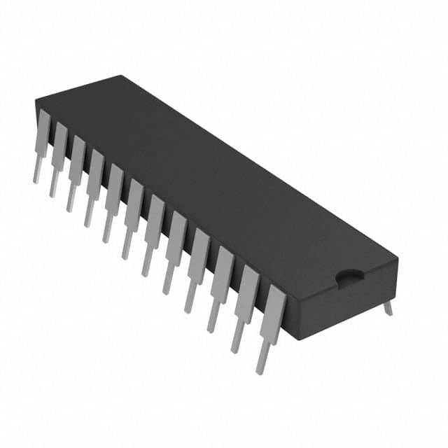
- Package: DIP (Dual In-line Package)
- Essence: CMOS Logic IC
- Packaging/Quantity: Tube/25 pieces
Specifications
- Supply Voltage Range: 3V to 18V
- Input Voltage Range: 0V to VDD
- Output Voltage Range: 0V to VDD
- Operating Temperature Range: -55°C to +125°C
- Propagation Delay Time: 100ns (max)
- Power Dissipation: 500mW (max)
Detailed Pin Configuration
The CD4508BE has a total of 16 pins. The pin configuration is as follows:
- A0 - Address Input 0
- A1 - Address Input 1
- A2 - Address Input 2
- A3 - Address Input 3
- E - Enable Input
- Y0 - Data Output 0
- Y1 - Data Output 1
- Y2 - Data Output 2
- Y3 - Data Output 3
- Y4 - Data Output 4
- Y5 - Data Output 5
- Y6 - Data Output 6
- Y7 - Data Output 7
- VSS - Ground
- VDD - Supply Voltage
- NC - No Connection
Functional Features
- 8-channel multiplexer/demultiplexer
- Low power consumption
- Wide supply voltage range
- High noise immunity
- Fast switching speed
- TTL and CMOS compatible inputs
- Break-before-make switching action
Advantages and Disadvantages
Advantages: - Versatile multiplexing/demultiplexing functionality - Low power consumption - Wide supply voltage range allows for compatibility with various systems - High noise immunity ensures reliable operation - Fast switching speed enables high-speed data processing
Disadvantages: - Limited number of channels (8) - Propagation delay time may affect timing-sensitive applications
Working Principles
The CD4508BE is a digital multiplexer/demultiplexer IC that allows the selection of one out of eight input lines to be routed to a single output line. It operates based on the principle of address decoding, where the binary address inputs (A0-A3) determine which input line is selected.
When the enable input (E) is high, the selected input is connected to the output line. When the enable input is low, the output is in a high impedance state. The IC is designed using CMOS technology, providing low power consumption and high noise immunity.
Detailed Application Field Plans
The CD4508BE can be used in various applications, including:
- Data communication systems
- Multiplexed data transmission
- Address decoding in microcontrollers
- Digital signal processing
- Analog-to-digital and digital-to-analog converters
- Industrial automation systems
- Test and measurement equipment
- Audio/video switchers
Detailed and Complete Alternative Models
Some alternative models to the CD4508BE include:
- CD4051B: 8-channel analog multiplexer/demultiplexer
- CD4052B: Dual 4-channel analog multiplexer/demultiplexer
- CD4053B: Triple 2-channel analog multiplexer/demultiplexer
- CD4051BCN: 8-channel analog multiplexer/demultiplexer (DIP package)
- CD74HC4067: 16-channel analog multiplexer/demultiplexer
These alternative models offer similar functionality and can be used as substitutes depending on specific requirements.
Word count: 389 words
Énumérez 10 questions et réponses courantes liées à l'application de CD4508BE dans les solutions techniques
Sure! Here are 10 common questions and answers related to the application of CD4508BE in technical solutions:
Q: What is CD4508BE? A: CD4508BE is a CMOS dual 4-bit latch/shift register IC (integrated circuit) commonly used in digital electronics.
Q: What are the main features of CD4508BE? A: CD4508BE features include parallel-to-serial or serial-to-parallel data conversion, latch enable inputs, and buffered outputs.
Q: How can CD4508BE be used in technical solutions? A: CD4508BE can be used for various applications such as data storage, data transfer, serial communication, and control systems.
Q: What is the maximum operating voltage for CD4508BE? A: The maximum operating voltage for CD4508BE is typically 15 volts.
Q: Can CD4508BE handle both positive and negative logic signals? A: Yes, CD4508BE is compatible with both positive and negative logic signals.
Q: Does CD4508BE require external components for operation? A: Yes, CD4508BE requires external resistors and capacitors for proper operation and stability.
Q: What is the power supply range for CD4508BE? A: The power supply range for CD4508BE is typically between 3 volts and 18 volts.
Q: Can CD4508BE be cascaded to increase the number of bits? A: Yes, CD4508BE can be cascaded to increase the number of bits by connecting the output of one IC to the input of another.
Q: Is CD4508BE suitable for high-speed applications? A: CD4508BE is not specifically designed for high-speed applications, but it can still be used in moderate-speed digital systems.
Q: Are there any alternative ICs to CD4508BE with similar functionality? A: Yes, some alternative ICs with similar functionality to CD4508BE include 74HC595, SN74LS164, and CD4015.
Please note that the answers provided here are general and may vary depending on specific datasheets and application requirements.