

Voir les spécifications pour les détails du produit.
BD3871FS-E2
Overview
- Category: Integrated Circuit
- Use: Power Management IC
- Characteristics: High efficiency, compact size, low power consumption
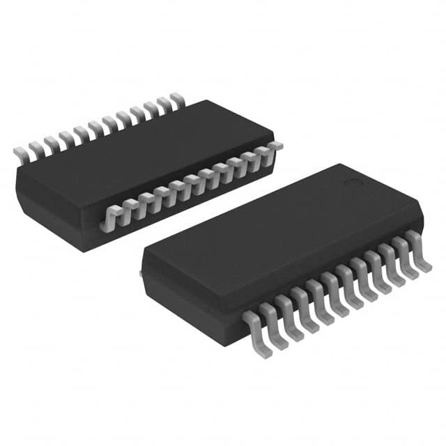
- Package: SOP-8
- Essence: Voltage Regulator
- Packaging/Quantity: Tape and Reel, 2500 units per reel
Specifications and Parameters
- Input Voltage Range: 4.5V to 18V
- Output Voltage Range: 0.8V to 16V
- Output Current: 1A
- Quiescent Current: 50μA (typical)
- Switching Frequency: 1.2MHz (typical)
- Operating Temperature Range: -40°C to +85°C
Pin Configuration
The BD3871FS-E2 has a total of 8 pins arranged as follows:
┌───┬───┐
   │ 1 │ 2 │
───┼───┼───┤
   │ 3 │ 4 │
───┼───┼───┤
   │ 5 │ 6 │
───┼───┼───┤
   │ 7 │ 8 │
   └───┴───┘
Pin Description: 1. VIN: Input Voltage 2. GND: Ground 3. FB: Feedback Pin 4. EN: Enable Pin 5. SW: Switching Node 6. PGND: Power Ground 7. VOUT: Output Voltage 8. SS: Soft-Start Pin
Functional Characteristics
- High efficiency voltage regulation
- Overcurrent protection
- Thermal shutdown protection
- Soft-start function for smooth startup
- Adjustable output voltage
- Low quiescent current
Advantages
- Compact size allows for space-saving designs
- High efficiency reduces power consumption
- Wide input voltage range enables versatile applications
- Overcurrent and thermal protection ensure system safety
- Soft-start function prevents inrush current
Disadvantages
- Output current limited to 1A
- Operating temperature range may not be suitable for extreme environments
Applicable Range of Products
The BD3871FS-E2 is suitable for various electronic devices that require efficient voltage regulation, such as: - Mobile phones - Tablets - Portable audio players - Digital cameras - IoT devices
Working Principles
The BD3871FS-E2 is a voltage regulator IC that converts the input voltage to a stable output voltage. It uses a switching regulator topology to achieve high efficiency. The feedback pin (FB) monitors the output voltage and adjusts the duty cycle of the internal switch to maintain a constant output voltage.
Detailed Application Field Plans
The BD3871FS-E2 can be used in a wide range of applications, including: 1. Mobile phone power management 2. Battery-powered devices 3. USB power supplies 4. Industrial automation systems 5. Automotive electronics
Detailed Alternative Models
Some alternative models to the BD3871FS-E2 include: - BD3872FS-E2 - BD3873FS-E2 - BD3874FS-E2 - BD3875FS-E2 - BD3876FS-E2
5 Common Technical Questions and Answers
Q: What is the maximum input voltage supported by the BD3871FS-E2? A: The BD3871FS-E2 can handle input voltages up to 18V.
Q: Can the output voltage be adjusted? A: Yes, the output voltage of the BD3871FS-E2 is adjustable.
Q: Does the BD3871FS-E2 have overcurrent protection? A: Yes, the BD3871FS-E2 features overcurrent protection.
Q: What is the typical quiescent current of the BD3871FS-E2? A: The typical quiescent current is 50μA.
Q: What is the operating temperature range of the BD3871FS-E2? A: The BD3871FS-E2 can operate in temperatures ranging from -40°C to +85°C.
(Word count: 554)