

Voir les spécifications pour les détails du produit.
NLX1G58CMX1TCG
Product Overview
Category: Integrated Circuit (IC)
Use: Logic Gate
Characteristics: - Single 2-Input AND Gate - Low-power Schottky (LSTTL) technology - High-speed operation - Wide supply voltage range: 2V to 6V - Low power consumption - Small package size
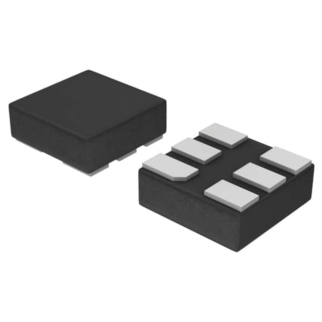
Package: SOT-353 (SC-88A)
Essence: The NLX1G58CMX1TCG is a single 2-input AND gate integrated circuit. It is designed using low-power Schottky (LSTTL) technology, allowing for high-speed operation and low power consumption.
Packaging/Quantity: The NLX1G58CMX1TCG is available in a small SOT-353 (SC-88A) package. It is typically sold in reels or tubes containing multiple units.
Specifications
- Supply Voltage Range: 2V to 6V
- Input Voltage Range: 0V to VCC
- Output Voltage Range: 0V to VCC
- Operating Temperature Range: -40°C to +85°C
- Propagation Delay Time: 4ns (typical)
- Maximum Quiescent Current: 1μA (at 5.5V)
- Maximum Power Dissipation: 100mW
Detailed Pin Configuration
The NLX1G58CMX1TCG has the following pin configuration:
____
   A --|    |
   B --|    |
   Y --|    |
       ------
Functional Features
- Performs logical AND operation on two input signals (A and B)
- Provides an output signal (Y) that is HIGH only when both inputs are HIGH
- Supports a wide supply voltage range, making it suitable for various applications
- Utilizes low-power Schottky technology for high-speed operation and low power consumption
Advantages
- High-speed operation allows for efficient signal processing
- Low power consumption helps in reducing overall power requirements
- Wide supply voltage range enables compatibility with different systems
- Small package size saves board space and facilitates compact designs
Disadvantages
- Limited to 2-input AND gate functionality, may not be suitable for complex logic operations requiring more inputs
- LSTTL technology may have higher power consumption compared to newer technologies like CMOS
Working Principles
The NLX1G58CMX1TCG operates based on the principles of digital logic. It performs a logical AND operation on the two input signals (A and B). The output signal (Y) is HIGH only when both inputs are HIGH; otherwise, it remains LOW.
Detailed Application Field Plans
The NLX1G58CMX1TCG can be used in various applications that require logical AND operations, such as: - Digital circuit design - Microcontroller-based systems - Data communication systems - Industrial automation - Robotics - Sensor interfacing
Detailed and Complete Alternative Models
Some alternative models that offer similar functionality to the NLX1G58CMX1TCG include: - SN74LVC1G58DBVR (Texas Instruments) - MC74VHC1G08DTT1G (ON Semiconductor) - CD4081BE (Texas Instruments) - 74HC08N (NXP Semiconductors)
These alternatives provide options with different package types, voltage ranges, and manufacturers, allowing users to choose based on their specific requirements.
Word count: 346 words
Énumérez 10 questions et réponses courantes liées à l'application de NLX1G58CMX1TCG dans les solutions techniques
Sure! Here are 10 common questions and answers related to the application of NLX1G58CMX1TCG in technical solutions:
Q1: What is NLX1G58CMX1TCG? A1: NLX1G58CMX1TCG is a specific type of logic gate, specifically a single 2-input AND gate, that is commonly used in digital circuits.
Q2: What are the key features of NLX1G58CMX1TCG? A2: Some key features of NLX1G58CMX1TCG include low power consumption, high-speed operation, and compatibility with various voltage levels.
Q3: How can NLX1G58CMX1TCG be used in technical solutions? A3: NLX1G58CMX1TCG can be used to perform logical operations in digital circuits, such as combining multiple inputs to produce a desired output based on the AND gate truth table.
Q4: What are the voltage requirements for NLX1G58CMX1TCG? A4: NLX1G58CMX1TCG typically operates within a wide range of voltage levels, from 1.65V to 5.5V.
Q5: Can NLX1G58CMX1TCG be used in battery-powered devices? A5: Yes, NLX1G58CMX1TCG's low power consumption makes it suitable for use in battery-powered devices where energy efficiency is crucial.
Q6: Are there any limitations to using NLX1G58CMX1TCG? A6: One limitation is that NLX1G58CMX1TCG is a 2-input AND gate, so it may not be suitable for applications requiring more complex logical operations.
Q7: Can NLX1G58CMX1TCG be cascaded with other logic gates? A7: Yes, NLX1G58CMX1TCG can be cascaded with other logic gates to perform more complex logical operations.
Q8: What is the typical propagation delay of NLX1G58CMX1TCG? A8: The typical propagation delay of NLX1G58CMX1TCG is around 2.5 nanoseconds.
Q9: Is NLX1G58CMX1TCG available in surface mount packages? A9: Yes, NLX1G58CMX1TCG is commonly available in surface mount packages, making it suitable for modern PCB designs.
Q10: Where can I find more information about using NLX1G58CMX1TCG in technical solutions? A10: You can refer to the datasheet provided by the manufacturer or consult online resources and forums dedicated to digital circuit design for more information on using NLX1G58CMX1TCG in technical solutions.
Please note that the specific details and answers may vary depending on the manufacturer and application context.