

Voir les spécifications pour les détails du produit.
NB3N121KMNG
Overview
- Category: Integrated Circuit
- Use: Clock Generator and Buffer
- Characteristics:
- Low power consumption
- Wide operating voltage range
- High frequency accuracy
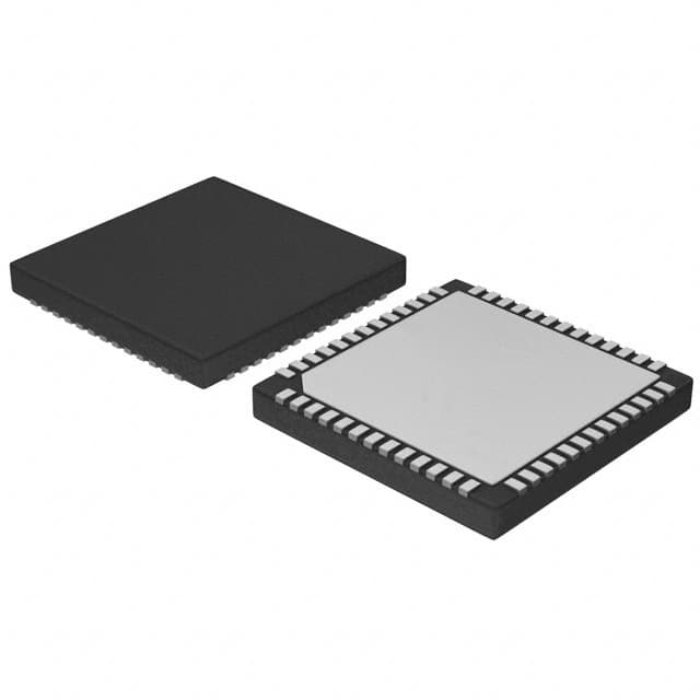
- Package: QFN (Quad Flat No-leads)
- Essence: Clock generation and buffering
- Packaging/Quantity: Tape and Reel, 3000 pieces per reel
Specifications and Parameters
- Supply Voltage: 1.8V to 3.3V
- Operating Temperature Range: -40°C to +85°C
- Output Frequency Range: 10MHz to 200MHz
- Output Type: LVCMOS
- Number of Outputs: 2
- Input Type: Crystal or LVCMOS
- Package Dimensions: 4mm x 4mm
Pin Configuration
The NB3N121KMNG has a total of 16 pins. The pin configuration is as follows:
- VDD
- GND
- OUT0
- OUT1
- OE
- SEL
- XTAL1
- XTAL2
- NC
- NC
- NC
- NC
- NC
- NC
- NC
- NC
Functional Characteristics
- Generates two clock outputs with selectable frequencies
- Supports crystal or LVCMOS input
- Output frequency can be programmed through the SEL pin
- Output enable/disable control through the OE pin
- Low jitter and phase noise
Advantages and Disadvantages
Advantages: - Wide operating voltage range allows for flexibility in different applications - Low power consumption helps conserve energy - High frequency accuracy ensures precise timing requirements
Disadvantages: - Limited number of outputs may not be suitable for complex systems requiring multiple clocks - Package size may limit its use in space-constrained designs
Applicable Range of Products
The NB3N121KMNG is suitable for various applications that require clock generation and buffering. Some examples include:
- Communication systems
- Networking equipment
- Consumer electronics
- Industrial automation
- Test and measurement instruments
Working Principles
The NB3N121KMNG utilizes an internal PLL (Phase-Locked Loop) to generate stable clock signals. It takes an input from either a crystal oscillator or LVCMOS signal and produces two output clocks with selectable frequencies. The output frequency can be programmed through the SEL pin, and the OE pin allows for enabling or disabling the outputs.
Detailed Application Field Plans
The NB3N121KMNG can be used in the following application fields:
- Ethernet Switches: Provides accurate clock signals for data transmission synchronization.
- Wireless Base Stations: Generates stable clock signals for wireless communication systems.
- Set-Top Boxes: Ensures precise timing for video and audio processing.
- Industrial Control Systems: Provides reliable clock signals for precise control and synchronization.
- Test Equipment: Offers accurate timing references for measurement instruments.
Detailed Alternative Models
Some alternative models to the NB3N121KMNG are:
- NB3N502: Similar clock generator and buffer with additional features.
- NB3N3002: Dual-channel clock generator with wider frequency range.
- NB3N2304: Clock generator with multiple outputs and programmable features.
5 Common Technical Questions and Answers
Q: What is the maximum operating voltage for the NB3N121KMNG? A: The maximum operating voltage is 3.3V.
Q: Can I use an external crystal oscillator as the input source? A: Yes, the NB3N121KMNG supports crystal or LVCMOS input.
Q: How many outputs does the NB3N121KMNG have? A: It has two clock outputs.
Q: Can I disable the clock outputs? A: Yes, the outputs can be enabled or disabled through the OE pin.
Q: What is the package size of the NB3N121KMNG? A: The package dimensions are 4mm x 4mm.
This concludes the encyclopedia entry for the NB3N121KMNG clock generator and buffer integrated circuit.