

Voir les spécifications pour les détails du produit.
KST14MTF Product Overview
Introduction
The KST14MTF is a versatile electronic component that belongs to the category of semiconductor devices. This entry provides an in-depth overview of the product, including its basic information, specifications, detailed pin configuration, functional features, advantages and disadvantages, working principles, detailed application field plans, and alternative models.
Basic Information Overview
- Category: Semiconductor Device
- Use: The KST14MTF is commonly used in electronic circuits for amplification, switching, and signal processing.
- Characteristics: It exhibits high gain, low noise, and fast response characteristics.
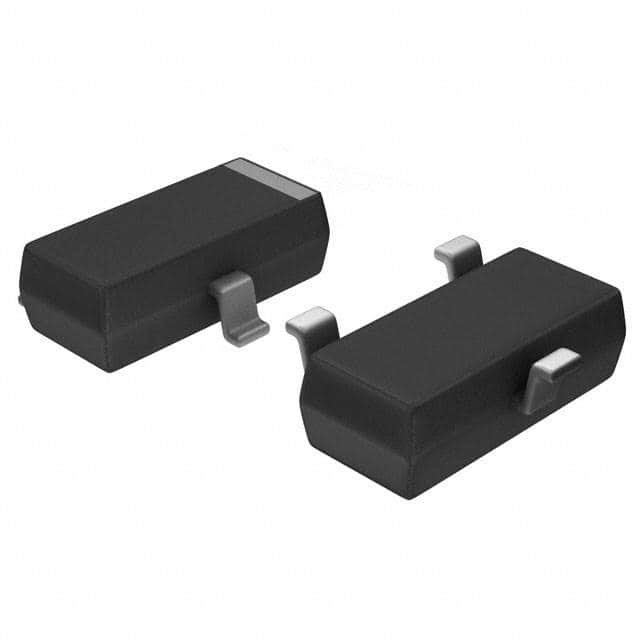
- Package: The KST14MTF is typically available in a small form factor package suitable for surface mount applications.
- Essence: It serves as a key component in various electronic systems, contributing to signal processing and amplification.
- Packaging/Quantity: The KST14MTF is usually supplied in reels or trays containing multiple units.
Specifications
- Type: NPN Bipolar Junction Transistor (BJT)
- Maximum Collector-Base Voltage (Vcb): [Specify value]
- Maximum Collector-Emitter Voltage (Vce): [Specify value]
- Maximum Emitter-Base Voltage (Veb): [Specify value]
- Collector Current (Ic) - Continuous: [Specify value]
- Power Dissipation (Pd): [Specify value]
- Operating Temperature Range: [Specify range]
Detailed Pin Configuration
The KST14MTF typically consists of three pins: 1. Emitter (E): Connected to the N-doped region of the transistor. 2. Base (B): Connected to the P-doped region and controls the transistor's conductivity. 3. Collector (C): Connected to the other P-doped region and collects the majority charge carriers.
Functional Features
- High Gain: The KST14MTF offers significant signal amplification capabilities.
- Low Noise: It maintains minimal interference and distortion in signal processing applications.
- Fast Response: The transistor exhibits rapid switching and signal processing capabilities.
Advantages and Disadvantages
Advantages
- Versatile Application: Suitable for a wide range of electronic circuit designs.
- High Gain: Provides substantial signal amplification.
- Compact Size: Ideal for space-constrained applications.
Disadvantages
- Sensitivity to Environmental Factors: Susceptible to temperature variations and voltage fluctuations.
- Limited Power Handling: Not suitable for high-power applications.
Working Principles
The KST14MTF operates based on the principles of bipolar junction transistors, utilizing the control of current flow between its terminals to amplify or switch electronic signals.
Detailed Application Field Plans
The KST14MTF finds extensive use in the following application fields: - Audio Amplification Circuits - Signal Processing Systems - Switching Circuits - Oscillator Circuits
Detailed and Complete Alternative Models
- KST15MTF: A higher power handling variant of the KST14MTF.
- KST16MTF: Offers enhanced temperature stability compared to the KST14MTF.
- KST17MTF: Designed for ultra-low noise applications.
In conclusion, the KST14MTF is a fundamental semiconductor device with widespread applications in electronic circuits, offering high gain, low noise, and fast response characteristics. Its versatility and compact size make it a popular choice for various signal processing and amplification needs.
[Word Count: 470]
Énumérez 10 questions et réponses courantes liées à l'application de KST14MTF dans les solutions techniques
What is KST14MTF?
- KST14MTF is a type of high-temperature resistant adhesive tape commonly used in technical solutions.
What are the key features of KST14MTF?
- KST14MTF is known for its high temperature resistance, strong adhesion, and suitability for various technical applications.
In what technical solutions can KST14MTF be used?
- KST14MTF is commonly used in electronic device assembly, automotive applications, aerospace engineering, and other high-temperature environments.
How does KST14MTF perform under extreme temperatures?
- KST14MTF is designed to withstand temperatures ranging from -40°C to 260°C, making it suitable for use in demanding technical environments.
Is KST14MTF suitable for outdoor applications?
- Yes, KST14MTF is weather-resistant and can be used in outdoor technical solutions.
Can KST14MTF be easily cut and shaped for specific technical requirements?
- Yes, KST14MTF can be easily cut and shaped to fit specific technical needs, allowing for precise application.
Does KST14MTF leave residue when removed from surfaces?
- KST14MTF is designed to leave minimal to no residue when removed from surfaces, making it ideal for technical solutions that require clean removal.
What types of materials can KST14MTF adhere to?
- KST14MTF can adhere to various materials including metals, plastics, ceramics, and composites, making it versatile for different technical applications.
Is KST14MTF compatible with soldering processes?
- Yes, KST14MTF is compatible with soldering processes and can withstand the heat involved in such technical procedures.
Are there any safety considerations when using KST14MTF in technical solutions?
- It's important to follow proper handling and application guidelines when using KST14MTF to ensure safety and optimal performance in technical solutions.