

Voir les spécifications pour les détails du produit.
FQB25N33TM - Semiconductor Device Encyclopedia Entry
Introduction
The FQB25N33TM is a semiconductor device belonging to the category of power MOSFETs. This entry provides an overview of its basic information, specifications, pin configuration, functional features, advantages and disadvantages, working principles, application field plans, and alternative models.
Basic Information Overview
- Category: Power MOSFET
- Use: The FQB25N33TM is commonly used in power supply applications, motor control, and other high-power switching circuits.
- Characteristics: It exhibits low on-resistance, high switching speed, and low gate charge, making it suitable for high-efficiency power conversion applications.
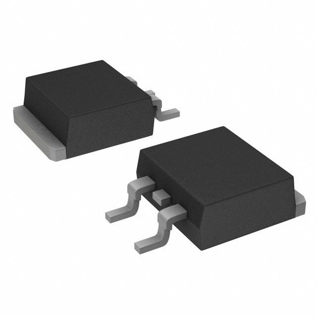
- Package: The device is typically available in a TO-263 package.
- Essence: Its essence lies in providing efficient power switching capabilities in various electronic circuits.
- Packaging/Quantity: The FQB25N33TM is usually packaged individually and is available in varying quantities based on manufacturer specifications.
Specifications
- Voltage Rating: 330V
- Current Rating: 25A
- On-Resistance: 0.15 ohms
- Gate-Source Voltage (Max): ±20V
- Package Type: TO-263
- Operating Temperature Range: -55°C to 175°C
Detailed Pin Configuration
The FQB25N33TM typically consists of three pins: 1. Gate (G): Input pin for controlling the switching operation. 2. Drain (D): The main terminal through which the current flows. 3. Source (S): The reference terminal for the device.
Functional Features
- High Efficiency: Due to its low on-resistance and gate charge, it enables high-efficiency power conversion.
- Fast Switching Speed: The device offers fast switching characteristics, making it suitable for high-frequency applications.
- Low Thermal Resistance: Helps in dissipating heat efficiently during operation.
Advantages and Disadvantages
Advantages
- High efficiency in power conversion applications.
- Fast switching speed enhances performance in high-frequency circuits.
- Low on-resistance minimizes power losses.
Disadvantages
- Sensitivity to voltage spikes and overcurrent conditions.
- Requires careful consideration of driving circuitry to avoid damage due to overvoltage or overcurrent situations.
Working Principles
The FQB25N33TM operates based on the principle of field-effect transistors, where the voltage applied to the gate terminal controls the flow of current between the drain and source terminals. By modulating the gate-source voltage, the device can be switched on and off rapidly, enabling efficient power control.
Detailed Application Field Plans
The FQB25N33TM finds extensive use in the following applications: - Power Supplies: Used in switch-mode power supplies for efficient voltage regulation. - Motor Control: Employed in motor drive circuits for precise control of motor speed and direction. - Inverters: Utilized in high-power inverters for converting DC to AC power in renewable energy systems.
Detailed and Complete Alternative Models
Some alternative models to the FQB25N33TM include: - IRF840: A similar power MOSFET with a voltage rating of 500V and a current rating of 8A. - STP55NF06L: Offers comparable performance with a voltage rating of 60V and a current rating of 50A.
In conclusion, the FQB25N33TM power MOSFET serves as a crucial component in various power electronics applications, offering high efficiency, fast switching, and reliable performance. Its specifications, functional features, and application field plans make it a versatile choice for power management and control circuits.
Word Count: 498
Énumérez 10 questions et réponses courantes liées à l'application de FQB25N33TM dans les solutions techniques
What is the maximum drain-source voltage of FQB25N33TM?
- The maximum drain-source voltage of FQB25N33TM is 330 volts.
What is the continuous drain current rating of FQB25N33TM?
- The continuous drain current rating of FQB25N33TM is 25 amperes.
What is the on-resistance of FQB25N33TM?
- The on-resistance of FQB25N33TM is typically 0.12 ohms.
Can FQB25N33TM be used in high-frequency applications?
- Yes, FQB25N33TM can be used in high-frequency applications due to its fast switching characteristics.
Is FQB25N33TM suitable for use in power supplies?
- Yes, FQB25N33TM is suitable for use in power supplies and DC-DC converters.
What is the operating temperature range of FQB25N33TM?
- The operating temperature range of FQB25N33TM is -55°C to 150°C.
Does FQB25N33TM require a heat sink for operation?
- It is recommended to use a heat sink with FQB25N33TM for efficient heat dissipation, especially at higher power levels.
Can FQB25N33TM be used in automotive applications?
- Yes, FQB25N33TM is suitable for automotive applications such as motor control and power management.
What type of package does FQB25N33TM come in?
- FQB25N33TM is available in a TO-263 (D2PAK) package.
Are there any application notes or reference designs available for using FQB25N33TM?
- Yes, application notes and reference designs are available from the manufacturer to assist in the proper implementation of FQB25N33TM in technical solutions.