

Voir les spécifications pour les détails du produit.
HEF4514BP,652
Product Overview
Category
HEF4514BP,652 belongs to the category of integrated circuits (ICs).
Use
This product is commonly used in digital electronics and microcontroller applications.
Characteristics
- HEF4514BP,652 is a 4-to-16 line decoder/demultiplexer.
- It has a wide operating voltage range of 3 V to 15 V.
- The device is designed to be compatible with most TTL families.
- It offers high noise immunity due to its Schmitt-trigger inputs.
- HEF4514BP,652 has a low power consumption.
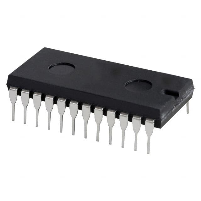
Package
The HEF4514BP,652 comes in a DIP (Dual In-line Package) format.
Essence
The essence of HEF4514BP,652 lies in its ability to decode a 4-bit binary input into one of sixteen mutually exclusive outputs.
Packaging/Quantity
This product is typically packaged in reels or tubes, with a quantity of 250 units per reel/tube.
Specifications
- Supply Voltage: 3 V to 15 V
- Input Voltage: 0 V to VDD
- Output Voltage: 0 V to VDD
- Operating Temperature Range: -40°C to +85°C
- Logic Family: CMOS
Detailed Pin Configuration
- GND (Ground)
- A0 (Input A0)
- A1 (Input A1)
- A2 (Input A2)
- A3 (Input A3)
- E (Enable Input)
- Y0 (Output Y0)
- Y1 (Output Y1)
- Y2 (Output Y2)
- Y3 (Output Y3)
- Y4 (Output Y4)
- Y5 (Output Y5)
- Y6 (Output Y6)
- Y7 (Output Y7)
- Y8 (Output Y8)
- Y9 (Output Y9)
- Y10 (Output Y10)
- Y11 (Output Y11)
- Y12 (Output Y12)
- Y13 (Output Y13)
- Y14 (Output Y14)
- Y15 (Output Y15)
- VDD (Positive Power Supply)
Functional Features
- HEF4514BP,652 is capable of decoding a 4-bit binary input into one of sixteen mutually exclusive outputs.
- It can be used as a demultiplexer to route data from a single input to any one of the sixteen outputs.
- The device offers high noise immunity and low power consumption.
Advantages and Disadvantages
Advantages
- Wide operating voltage range allows for compatibility with various systems.
- High noise immunity ensures reliable operation in noisy environments.
- Low power consumption helps conserve energy.
Disadvantages
- Limited number of inputs and outputs restricts its application in complex systems.
- Lack of built-in protection features may make it susceptible to damage from voltage spikes or other electrical disturbances.
Working Principles
HEF4514BP,652 operates based on the principle of binary decoding. The four input lines (A0, A1, A2, A3) represent a binary code, which is decoded to activate one of the sixteen output lines (Y0 to Y15). The enable input (E) controls the activation of the decoder/demultiplexer.
Detailed Application Field Plans
HEF4514BP,652 finds applications in various fields, including: 1. Digital electronics 2. Microcontroller-based systems 3. Data routing and selection circuits 4. Address decoding in memory systems 5. Multiplexing and demultiplexing applications
Detailed and Complete Alternative Models
Some alternative models to HEF4514BP,652 include: 1. CD4514BE 2. SN74LS154N 3. MC14514BCP 4. 74HC154N 5. CD74HC154E
These alternative models offer similar functionality and can be used as substitutes for HEF4514BP,652 in various applications.
Word count: 536 words
Énumérez 10 questions et réponses courantes liées à l'application de HEF4514BP,652 dans les solutions techniques
Sure! Here are 10 common questions and answers related to the application of HEF4514BP,652:
Q: What is the HEF4514BP,652? A: The HEF4514BP,652 is a 4-to-16 line decoder/demultiplexer IC (integrated circuit) commonly used in digital electronics.
Q: What is the purpose of the HEF4514BP,652? A: The purpose of this IC is to decode a 4-bit binary input and activate one of the 16 output lines based on the input value.
Q: How does the HEF4514BP,652 work? A: The IC uses internal logic gates to decode the binary input and activate the corresponding output line by driving it to a low voltage level.
Q: What is the maximum input voltage for the HEF4514BP,652? A: The maximum input voltage for this IC is typically around 5.5V.
Q: Can the HEF4514BP,652 be used with both TTL and CMOS logic levels? A: Yes, this IC is compatible with both TTL (Transistor-Transistor Logic) and CMOS (Complementary Metal-Oxide-Semiconductor) logic levels.
Q: What is the maximum output current of the HEF4514BP,652? A: The maximum output current per output pin is typically around 6 mA.
Q: Can the HEF4514BP,652 be cascaded to increase the number of outputs? A: Yes, multiple HEF4514BP,652 ICs can be cascaded together to increase the number of available outputs.
Q: What is the power supply voltage range for the HEF4514BP,652? A: The power supply voltage range for this IC is typically between 3V and 18V.
Q: Can the HEF4514BP,652 be used in both digital and analog applications? A: No, this IC is primarily designed for digital applications and may not be suitable for analog applications.
Q: Are there any specific precautions to consider when using the HEF4514BP,652? A: It is important to ensure that the power supply voltage does not exceed the specified range and to follow the recommended operating conditions provided in the datasheet to ensure proper functionality and reliability of the IC.