

Voir les spécifications pour les détails du produit.
Encyclopedia Entry: 74LVT241BQ,115
Product Overview
Category
The 74LVT241BQ,115 belongs to the category of integrated circuits (ICs) and specifically falls under the family of logic gates.
Use
This product is commonly used in digital electronics for signal processing and data manipulation. It serves as a buffer/line driver with 3-state outputs.
Characteristics
- Low voltage operation: The 74LVT241BQ,115 operates at low voltage levels, typically between 2.7V and 3.6V.
- High-speed performance: It offers fast propagation delay times, making it suitable for high-frequency applications.
- 3-state outputs: The device features three output states - high, low, and high impedance - allowing multiple devices to share a common bus.
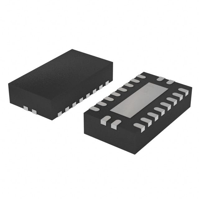
Package
The 74LVT241BQ,115 is available in a small-outline package (SOIC). This package type provides ease of handling and compatibility with automated assembly processes.
Essence
The essence of this product lies in its ability to provide reliable signal buffering and driving capabilities while operating at low voltages.
Packaging/Quantity
The 74LVT241BQ,115 is typically packaged in reels or tubes, containing a specific quantity of ICs per package. The exact packaging and quantity may vary depending on the manufacturer.
Specifications
- Supply Voltage Range: 2.7V to 3.6V
- Input Voltage Range: 0V to VCC
- Output Voltage Range: 0V to VCC
- Operating Temperature Range: -40°C to +85°C
- Logic Family: LVT
- Number of Inputs: 8
- Number of Outputs: 8
- Output Type: 3-state
Detailed Pin Configuration
The 74LVT241BQ,115 has a total of 20 pins, each serving a specific function. The pin configuration is as follows:
- Output Y1
- Output Y2
- Output Y3
- Output Y4
- Output Y5
- Output Y6
- Output Y7
- Output Y8
- GND (Ground)
- Input G
- Input A1
- Input A2
- Input A3
- Input A4
- VCC (Supply Voltage)
- Output Enable (OE)
- Input B1
- Input B2
- Input B3
- Input B4
Functional Features
- Buffering: The 74LVT241BQ,115 acts as a buffer, amplifying and stabilizing digital signals.
- Line Driving: It provides the capability to drive signals over longer distances without significant degradation.
- 3-State Outputs: The device offers three output states - high, low, and high impedance - allowing for efficient bus sharing.
Advantages and Disadvantages
Advantages
- Low voltage operation enables compatibility with modern low-power systems.
- High-speed performance allows for quick signal processing.
- 3-state outputs facilitate efficient bus sharing in multi-device systems.
Disadvantages
- Limited input/output count may restrict its use in complex applications.
- Requires external components for proper functionality.
Working Principles
The 74LVT241BQ,115 operates based on the principles of digital logic gates. It receives input signals from the A and B inputs and processes them using internal circuitry. The output signals are then amplified and driven through the Y outputs. The OE pin controls the output enable/disable functionality.
Detailed Application Field Plans
The 74LVT241BQ,115 finds applications in various fields, including but not limited to: - Microprocessor systems - Data communication networks - Industrial automation - Consumer electronics
Detailed and Complete Alternative Models
Some alternative models that offer similar functionality to the 74LVT241BQ,115 include: - 74LVTH241 - SN74LVC1G241 - MC74VHC541
These alternatives can be considered based on specific requirements and compatibility with existing systems.
In conclusion, the 74LVT241BQ,115 is a versatile integrated circuit used for signal buffering and driving in digital electronics. Its low voltage operation, high-speed performance, and 3-state outputs make it suitable for various applications. However, its limited input/output count and external component requirement should be taken into consideration when selecting this product for specific projects.
Énumérez 10 questions et réponses courantes liées à l'application de 74LVT241BQ,115 dans les solutions techniques
Sure! Here are 10 common questions and answers related to the application of 74LVT241BQ,115:
1. What is the function of the 74LVT241BQ,115? The 74LVT241BQ,115 is an octal buffer/line driver with 3-state outputs. It is used for driving high-capacitance loads while maintaining low power consumption.
2. What is the maximum operating voltage for the 74LVT241BQ,115? The maximum operating voltage for the 74LVT241BQ,115 is 3.6V.
3. How many inputs does the 74LVT241BQ,115 have? The 74LVT241BQ,115 has 8 inputs.
4. Can the 74LVT241BQ,115 be used in both CMOS and TTL applications? Yes, the 74LVT241BQ,115 is compatible with both CMOS and TTL logic levels.
5. What is the output current capability of the 74LVT241BQ,115? The 74LVT241BQ,115 has a typical output current capability of ±32mA.
6. Does the 74LVT241BQ,115 have internal pull-up or pull-down resistors? No, the 74LVT241BQ,115 does not have internal pull-up or pull-down resistors.
7. Can the 74LVT241BQ,115 be used in high-speed applications? Yes, the 74LVT241BQ,115 is designed for high-speed operation and can be used in such applications.
8. What is the propagation delay of the 74LVT241BQ,115? The propagation delay of the 74LVT241BQ,115 is typically 3.5ns.
9. Is the 74LVT241BQ,115 suitable for bidirectional data transfer? No, the 74LVT241BQ,115 is a unidirectional buffer and does not support bidirectional data transfer.
10. Can the 74LVT241BQ,115 be used in automotive applications? Yes, the 74LVT241BQ,115 is qualified for automotive applications and can be used in such environments.
Please note that these answers are general and may vary depending on the specific datasheet and application requirements.