

Voir les spécifications pour les détails du produit.
74LVC1G07GV,125
Basic Information Overview
- Category: Integrated Circuit (IC)
- Use: Logic Buffer/Driver
- Characteristics: Single Buffer with Open Drain Output, Low Voltage CMOS Technology
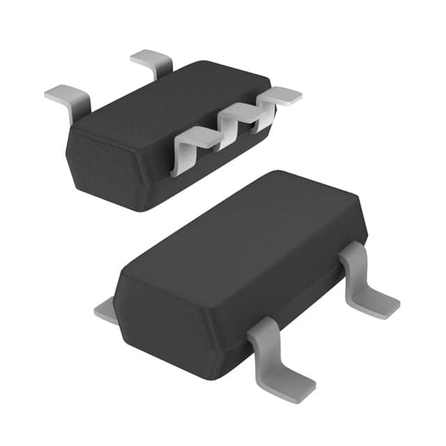
- Package: SOT753 (SC-70)
- Essence: High-Speed CMOS Buffer with Open Drain Output
- Packaging/Quantity: Tape and Reel, 3000 pieces per reel
Specifications
- Supply Voltage Range: 1.65V to 5.5V
- Input Voltage Range: -0.5V to VCC + 0.5V
- Output Voltage Range: 0V to VCC
- Maximum Operating Frequency: 400 MHz
- Maximum Propagation Delay: 4.3 ns
- Maximum Output Current: ±32 mA
- Operating Temperature Range: -40°C to +125°C
Detailed Pin Configuration
The 74LVC1G07GV,125 IC has the following pin configuration:
____
   A1 |    | VCC
   A2 |    | Y
  GND |____| B1
Functional Features
- Single buffer with open drain output
- Compatible with wide voltage range from 1.65V to 5.5V
- High-speed operation up to 400 MHz
- Low power consumption
- Provides level shifting capability
- Supports bidirectional data flow
Advantages
- Small package size allows for space-saving designs
- Wide operating voltage range enables compatibility with various systems
- High-speed operation facilitates fast data transmission
- Low power consumption helps in energy-efficient applications
- Level shifting capability enhances compatibility between different voltage domains
- Bidirectional data flow support adds flexibility to the design
Disadvantages
- Limited output current capacity compared to some other buffer/driver ICs
- Open drain output requires external pull-up resistor for proper operation
Working Principles
The 74LVC1G07GV,125 is a logic buffer/driver IC that amplifies and controls the voltage levels of digital signals. It utilizes low voltage CMOS technology to achieve high-speed operation while consuming minimal power. The open drain output allows bidirectional data flow and requires an external pull-up resistor to provide a logical high level.
Detailed Application Field Plans
The 74LVC1G07GV,125 can be used in various applications, including but not limited to: - Level shifting in mixed-voltage systems - I2C bus interface - General-purpose logic buffering - Signal amplification and shaping - Voltage translation between different domains
Detailed and Complete Alternative Models
Some alternative models that offer similar functionality to the 74LVC1G07GV,125 are: - SN74LVC1G07DBVR (Texas Instruments) - MC74VHC1GT07DTT1G (ON Semiconductor) - NC7SZ07P5X (Fairchild Semiconductor) - TC7SZ07FU(T5L,F) (Toshiba)
Please note that the above list is not exhaustive, and there may be other alternative models available from different manufacturers.
Word count: 347 words
Énumérez 10 questions et réponses courantes liées à l'application de 74LVC1G07GV,125 dans les solutions techniques
Sure! Here are 10 common questions and answers related to the application of 74LVC1G07GV,125 in technical solutions:
Q1: What is the 74LVC1G07GV,125? A1: The 74LVC1G07GV,125 is a single buffer/driver with open-drain output. It is commonly used in digital logic circuits.
Q2: What is the voltage supply range for the 74LVC1G07GV,125? A2: The voltage supply range for the 74LVC1G07GV,125 is typically between 1.65V and 5.5V.
Q3: What is the maximum output current of the 74LVC1G07GV,125? A3: The maximum output current of the 74LVC1G07GV,125 is typically around 32mA.
Q4: Can the 74LVC1G07GV,125 be used as a level shifter? A4: Yes, the 74LVC1G07GV,125 can be used as a level shifter to convert signals between different voltage levels.
Q5: What is the maximum operating frequency of the 74LVC1G07GV,125? A5: The maximum operating frequency of the 74LVC1G07GV,125 is typically around 500MHz.
Q6: Is the 74LVC1G07GV,125 compatible with both CMOS and TTL logic levels? A6: Yes, the 74LVC1G07GV,125 is compatible with both CMOS and TTL logic levels.
Q7: Can the 74LVC1G07GV,125 be used in bidirectional communication? A7: No, the 74LVC1G07GV,125 is a unidirectional buffer/driver and cannot be used for bidirectional communication.
Q8: What is the typical propagation delay of the 74LVC1G07GV,125? A8: The typical propagation delay of the 74LVC1G07GV,125 is around 4.5ns.
Q9: Can the 74LVC1G07GV,125 drive capacitive loads? A9: Yes, the 74LVC1G07GV,125 can drive capacitive loads up to a certain limit specified in the datasheet.
Q10: Is the 74LVC1G07GV,125 available in different package options? A10: Yes, the 74LVC1G07GV,125 is available in various package options such as SOT23, SC-88, and XSON.