

Voir les spécifications pour les détails du produit.
74LVC162244ADL,112
Basic Information Overview
- Category: Integrated Circuit (IC)
- Use: Logic Level Shifter
- Characteristics: High-speed, low-power, bidirectional voltage translation between different logic levels
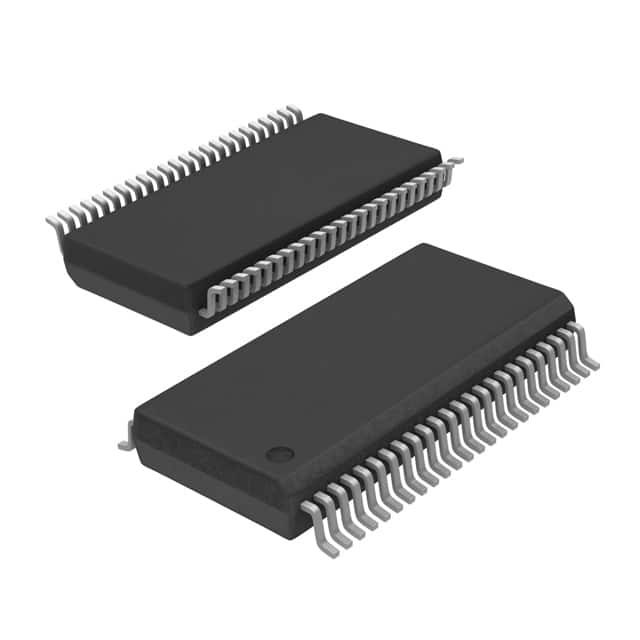
- Package: TSSOP (Thin Shrink Small Outline Package)
- Essence: Voltage level shifting and signal buffering
- Packaging/Quantity: Tape and Reel, 2500 units per reel
Specifications
- Number of Channels: 16
- Input Voltage Range: 1.2V to 3.6V
- Output Voltage Range: 1.2V to 3.6V
- Maximum Data Rate: 400 Mbps
- Supply Voltage Range: 1.65V to 3.6V
- Operating Temperature Range: -40°C to +85°C
Detailed Pin Configuration
The 74LVC162244ADL,112 has a total of 48 pins, divided into two groups of 24 pins each. Each group corresponds to one direction of voltage translation. The pin configuration is as follows:
Group A (Direction A to B)
- OE (Output Enable) A1
- I/O1A A2
- GND A3
- I/O2A A4
- VCC A5
- I/O3A A6
- GND A7
- I/O4A A8
- I/O5A A9
- GND A10
- I/O6A A11
- VCC A12
- I/O7A A13
- GND A14
- I/O8A A15
- I/O9A A16
- GND A17
- I/O10A A18
- VCC A19
- I/O11A A20
- GND A21
- I/O12A A22
- I/O13A A23
- GND A24
Group B (Direction B to A)
- OE (Output Enable) B1
- I/O1B B2
- GND B3
- I/O2B B4
- VCC B5
- I/O3B B6
- GND B7
- I/O4B B8
- I/O5B B9
- GND B10
- I/O6B B11
- VCC B12
- I/O7B B13
- GND B14
- I/O8B B15
- I/O9B B16
- GND B17
- I/O10B B18
- VCC B19
- I/O11B B20
- GND B21
- I/O12B B22
- I/O13B B23
- GND B24
Functional Features
- Bidirectional voltage translation: Allows for seamless communication between devices operating at different logic levels.
- High-speed operation: Supports data rates up to 400 Mbps, enabling fast signal transmission.
- Low-power consumption: Designed to minimize power consumption, making it suitable for battery-powered applications.
- Output enable control: The OE pin allows for disabling the outputs, providing flexibility in controlling the direction of data flow.
Advantages and Disadvantages
Advantages: - Efficient voltage level shifting between different logic levels. - High-speed operation for fast data transmission. - Low-power consumption for energy-efficient applications. - Compact TSSOP package for space-constrained designs.
Disadvantages: - Limited number of channels (16) compared to other logic level shifters. - Restricted voltage range (1.2V to 3.6V) may not be suitable for all applications.
Working Principles
The 74LVC162244ADL,112 utilizes a combination of MOSFETs and CMOS technology to achieve bidirectional voltage translation. It employs a voltage level shifting technique that allows signals to be translated from one logic level to another while maintaining signal integrity and minimizing power consumption. The OE pin controls the direction of data flow by enabling or disabling the outputs.
Detailed Application Field Plans
The 74LVC162244ADL,112 is commonly used in various applications where voltage level shifting is required. Some typical application fields include: - Communication systems: Facilitates communication between devices operating at different logic levels, such as microcontrollers, sensors, and display modules. - Industrial automation: Enables seamless integration of components with different voltage requirements, enhancing system compatibility and reliability. - Consumer electronics: Used in devices like smartphones, tablets, and gaming consoles to interface between different logic level
Énumérez 10 questions et réponses courantes liées à l'application de 74LVC162244ADL,112 dans les solutions techniques
Sure! Here are 10 common questions and answers related to the application of 74LVC162244ADL,112 in technical solutions:
Q: What is the function of the 74LVC162244ADL,112? A: The 74LVC162244ADL,112 is a 16-bit buffer/driver with 3-state outputs. It can be used to amplify and control signals in digital circuits.
Q: What is the voltage range supported by the 74LVC162244ADL,112? A: The 74LVC162244ADL,112 supports a voltage range of 1.65V to 5.5V.
Q: How many channels does the 74LVC162244ADL,112 have? A: The 74LVC162244ADL,112 has 16 channels, each capable of buffering a single bit.
Q: Can the 74LVC162244ADL,112 handle high-speed data transmission? A: Yes, the 74LVC162244ADL,112 is designed for high-speed operation and can handle fast data transmission.
Q: What is the maximum output current of the 74LVC162244ADL,112? A: The 74LVC162244ADL,112 can provide a maximum output current of 24mA per channel.
Q: Is the 74LVC162244ADL,112 compatible with both TTL and CMOS logic levels? A: Yes, the 74LVC162244ADL,112 is compatible with both TTL and CMOS logic levels, making it versatile for various applications.
Q: Can the 74LVC162244ADL,112 be used for bidirectional data transfer? A: Yes, the 74LVC162244ADL,112 supports bidirectional data flow, allowing it to be used for both input and output operations.
Q: What is the power supply voltage required for the 74LVC162244ADL,112? A: The 74LVC162244ADL,112 requires a power supply voltage of 2.7V to 3.6V.
Q: Does the 74LVC162244ADL,112 have built-in protection features? A: Yes, the 74LVC162244ADL,112 has built-in ESD protection on all inputs and outputs, ensuring reliability in harsh environments.
Q: Can multiple 74LVC162244ADL,112 chips be cascaded together? A: Yes, multiple 74LVC162244ADL,112 chips can be cascaded together to expand the number of channels or create larger buffer arrays.
Please note that these answers are general and may vary depending on the specific application and requirements.