Voir les spécifications pour les détails du produit.

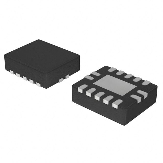
74LVC08ABQ,115
Basic Information Overview
- Category: Integrated Circuit (IC)
- Use: Logic Gate
- Characteristics: Low-voltage CMOS Quad 2-input AND gate
- Package: 14-pin plastic small outline package (SOT108-1)
- Essence: This IC is a logic gate that performs the AND operation on two input signals.
- Packaging/Quantity: Available in reels of 2500 units
Specifications
- Supply Voltage Range: 1.65V to 5.5V
- High-level Input Voltage: 0.7 x VCC
- Low-level Input Voltage: 0.3 x VCC
- High-level Output Current: -32 mA
- Low-level Output Current: 32 mA
- Propagation Delay: 4.3 ns (typical)
Detailed Pin Configuration
The 74LVC08ABQ,115 IC has a total of 14 pins. The pin configuration is as follows:
+---+--+---+
   A1 |1      14| VCC
   B1 |2      13| A4
   Y1 |3      12| B4
   A2 |4      11| Y4
   B2 |5      10| GND
   Y2 |6       9| A3
   A1 |7       8| B3
       +--------+
Functional Features
- Quad 2-input AND gate: The IC contains four independent AND gates, each with two inputs and one output.
- Low-voltage operation: It operates at a low voltage range of 1.65V to 5.5V, making it suitable for battery-powered devices.
- CMOS technology: The IC utilizes Complementary Metal-Oxide-Semiconductor (CMOS) technology, providing low power consumption and high noise immunity.
- Fast propagation delay: With a typical propagation delay of 4.3 ns, it ensures quick response in digital logic circuits.
Advantages and Disadvantages
Advantages: - Low-voltage operation allows for compatibility with various systems. - CMOS technology provides low power consumption and high noise immunity. - Compact package size enables space-saving designs. - Fast propagation delay ensures efficient signal processing.
Disadvantages: - Limited number of gates per IC may require multiple ICs for complex logic operations. - Not suitable for high-voltage applications.
Working Principles
The 74LVC08ABQ,115 is based on CMOS technology, which utilizes both NMOS and PMOS transistors to implement logic functions. In the case of the AND gate, the output is high only when both inputs are high. The internal circuitry of the IC ensures proper logical operation by controlling the flow of current through the transistors based on the input signals.
Detailed Application Field Plans
The 74LVC08ABQ,115 IC finds applications in various digital logic circuits, including but not limited to: - Microcontrollers and microprocessors - Data communication systems - Industrial automation - Consumer electronics - Automotive electronics
Detailed and Complete Alternative Models
Some alternative models that can be used as substitutes for the 74LVC08ABQ,115 IC include: - SN74LVC08A from Texas Instruments - MC74VHC1G08 from ON Semiconductor - CD4081B from Texas Instruments - HCF4081B from STMicroelectronics - 74HC08 from NXP Semiconductors
Note: These alternative models may have slight variations in specifications and pin configuration, so careful consideration should be given to ensure compatibility with the specific application requirements.
Word count: 409
Énumérez 10 questions et réponses courantes liées à l'application de 74LVC08ABQ,115 dans les solutions techniques
Sure! Here are 10 common questions and answers related to the application of 74LVC08ABQ,115 in technical solutions:
Question: What is the 74LVC08ABQ,115?
Answer: The 74LVC08ABQ,115 is a quad 2-input AND gate integrated circuit (IC) that operates on low-voltage CMOS technology.Question: What is the operating voltage range for the 74LVC08ABQ,115?
Answer: The operating voltage range for this IC is typically between 1.65V and 5.5V.Question: What is the maximum output current of the 74LVC08ABQ,115?
Answer: The maximum output current per gate is around 32mA.Question: Can the 74LVC08ABQ,115 be used in both digital and analog applications?
Answer: No, this IC is specifically designed for digital applications and is not suitable for analog use.Question: What is the propagation delay of the 74LVC08ABQ,115?
Answer: The typical propagation delay for this IC is around 3.8ns.Question: Can the 74LVC08ABQ,115 be used in high-speed applications?
Answer: Yes, this IC is suitable for high-speed applications due to its low propagation delay and fast switching characteristics.Question: Is the 74LVC08ABQ,115 compatible with other logic families?
Answer: Yes, it is compatible with both TTL and CMOS logic families, making it versatile for various applications.Question: What is the power dissipation of the 74LVC08ABQ,115?
Answer: The power dissipation of this IC is typically around 1.8mW per gate.Question: Can the 74LVC08ABQ,115 be used in battery-powered devices?
Answer: Yes, it can be used in battery-powered devices due to its low power consumption and wide operating voltage range.Question: Are there any specific precautions to consider when using the 74LVC08ABQ,115?
Answer: It is important to avoid exceeding the maximum ratings specified in the datasheet, such as voltage and temperature limits, to ensure proper functionality and reliability of the IC.

