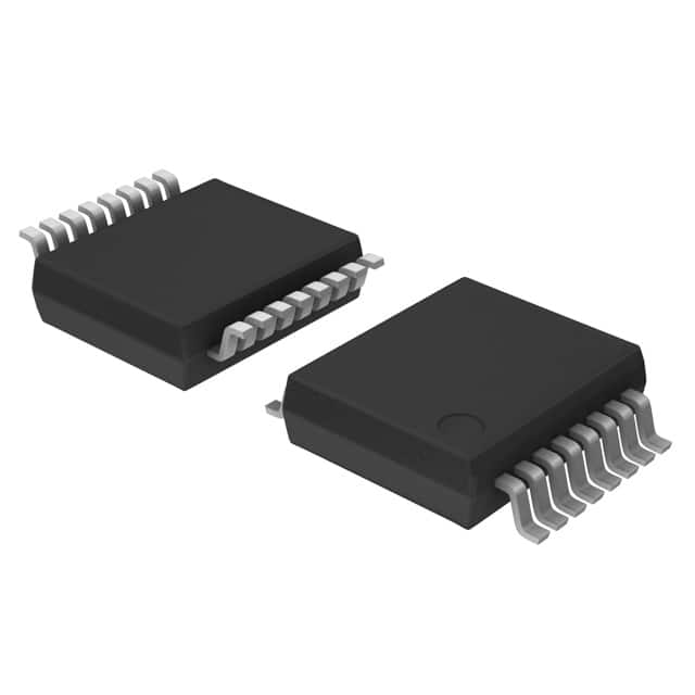
Voir les spécifications pour les détails du produit.

74LV138DB,118
Basic Information Overview
- Category: Integrated Circuit (IC)
- Use: Decoder/Demultiplexer
- Characteristics: Low-voltage, low-power, high-speed operation
- Package: SSOP (Shrink Small Outline Package)
- Essence: Digital logic decoder/demultiplexer
- Packaging/Quantity: Tape and reel, 2500 units per reel
Specifications
- Supply Voltage Range: 1.65V to 5.5V
- Input Voltage Range: -0.5V to VCC + 0.5V
- Output Voltage Range: -0.5V to VCC + 0.5V
- Operating Temperature Range: -40°C to +125°C
- Logic Family: LV (Low-Voltage)
Detailed Pin Configuration
The 74LV138DB,118 IC has a total of 16 pins. The pin configuration is as follows:
┌───┐
   A3 ─┤1  16├─ VCC
   A2 ─┤2  15├─ Y0
   A1 ─┤3  14├─ Y1
   A0 ─┤4  13├─ Y2
  /G1 ─┤5  12├─ GND
  /G2A ─┤6  11├─ Y3
  /G2B ─┤7  10├─ Y4
  /Y3 ─┤8   9├─ Y5
        └───┘
Functional Features
- Decodes three binary address inputs (A0, A1, A2) into eight mutually exclusive outputs (Y0-Y7).
- Enables the selected output based on the input address.
- Low-voltage operation allows compatibility with a wide range of digital systems.
- Low-power consumption makes it suitable for battery-powered devices.
- High-speed operation ensures efficient data processing.
Advantages and Disadvantages
Advantages: - Compact SSOP package saves board space. - Wide supply voltage range enhances versatility. - Low power consumption extends battery life. - High-speed operation enables quick data decoding.
Disadvantages: - Limited number of address inputs restricts the range of applications. - Not suitable for high-voltage applications.
Working Principles
The 74LV138DB,118 is a decoder/demultiplexer IC that converts binary address inputs into mutually exclusive outputs. The three address inputs (A0, A1, A2) determine which output (Y0-Y7) is enabled. When the enable inputs (/G1, /G2A, /G2B) are active low, the selected output is activated. The IC operates at low voltages and consumes minimal power while providing high-speed operation.
Detailed Application Field Plans
The 74LV138DB,118 IC finds applications in various fields, including: 1. Digital electronics: Used in microcontrollers, programmable logic devices, and digital signal processors for address decoding. 2. Communication systems: Employed in multiplexers, routers, and switches for channel selection and data routing. 3. Consumer electronics: Integrated into remote controls, set-top boxes, and audio/video equipment for signal demultiplexing. 4. Automotive industry: Utilized in automotive control units, infotainment systems, and dashboard displays for address decoding and signal routing.
Detailed and Complete Alternative Models
Some alternative models to the 74LV138DB,118 IC include: - 74HC138: High-speed CMOS version with similar functionality. - CD74HC138: High-speed CMOS decoder/demultiplexer from Texas Instruments. - SN74LS138: Low-power Schottky TTL version with similar functionality.
(Note: The above list is not exhaustive and serves as an example of alternative models.)
In conclusion, the 74LV138DB,118 is a low-voltage decoder/demultiplexer IC that offers high-speed operation and low power consumption. Its compact package and wide supply voltage range make it suitable for various digital applications. However, its limited address inputs and unsuitability for high-voltage applications are notable limitations.
Énumérez 10 questions et réponses courantes liées à l'application de 74LV138DB,118 dans les solutions techniques
Sure! Here are 10 common questions and answers related to the application of 74LV138DB,118 in technical solutions:
Q: What is the 74LV138DB,118? A: The 74LV138DB,118 is a 3-to-8 line decoder/demultiplexer IC (integrated circuit) commonly used in digital electronics.
Q: What is the purpose of a decoder/demultiplexer? A: A decoder/demultiplexer takes an input signal and selects one of several output lines based on the input value.
Q: How many inputs does the 74LV138DB,118 have? A: The 74LV138DB,118 has three inputs (A0, A1, and A2) which can be used to select one of eight output lines.
Q: What is the maximum voltage the 74LV138DB,118 can handle? A: The 74LV138DB,118 can handle a maximum voltage of 5.5V.
Q: How many output lines does the 74LV138DB,118 have? A: The 74LV138DB,118 has eight output lines (Y0-Y7).
Q: Can the 74LV138DB,118 be used for both decoding and demultiplexing? A: Yes, the 74LV138DB,118 can be used for both decoding and demultiplexing applications.
Q: What is the typical power supply voltage for the 74LV138DB,118? A: The typical power supply voltage for the 74LV138DB,118 is 3.3V.
Q: What is the maximum operating frequency of the 74LV138DB,118? A: The maximum operating frequency of the 74LV138DB,118 is typically around 125 MHz.
Q: Can the 74LV138DB,118 be cascaded to increase the number of output lines? A: Yes, multiple 74LV138DB,118 ICs can be cascaded together to increase the number of output lines.
Q: What are some common applications of the 74LV138DB,118? A: The 74LV138DB,118 is commonly used in address decoding, memory selection, and general-purpose digital logic circuits.
Please note that these answers are general and may vary depending on specific use cases and requirements.

