

Voir les spécifications pour les détails du produit.
74HCT2G66GD,125
Basic Information Overview
- Category: Integrated Circuit (IC)
- Use: Digital Logic Switch
- Characteristics: High-speed, low-power, dual bilateral switch
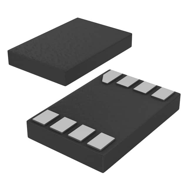
- Package: SOT353 (Thin Shrink Small Outline Package)
- Essence: Transistor-Transistor Logic (TTL) compatible CMOS technology
- Packaging/Quantity: Tape and Reel, 3000 pieces per reel
Specifications
- Supply Voltage Range: 2.0V to 5.5V
- High-Level Input Voltage: 2.0V to VCC
- Low-Level Input Voltage: GND to 0.8V
- High-Level Output Voltage: VCC - 0.4V
- Low-Level Output Voltage: 0.1V
- Maximum Continuous Current through Each Switch: ±25mA
- Maximum Continuous Current through VCC or GND: ±50mA
- Operating Temperature Range: -40°C to +125°C
Detailed Pin Configuration
The 74HCT2G66GD,125 has a total of 8 pins arranged as follows:
____
   1 |o    | 8
   2 |     | 7
   3 |     | 6
   4 |_____| 5
Pin Description: 1. A1: Control input for switch 1 2. B1: Control input for switch 2 3. Y1: Output for switch 1 4. Y2: Output for switch 2 5. GND: Ground 6. Y2: Output for switch 2 7. B1: Control input for switch 2 8. A1: Control input for switch 1
Functional Features
- Dual Bilateral Switch: Allows bidirectional signal transmission
- TTL Compatible: Can interface with TTL logic levels
- Low Power Consumption: Suitable for battery-powered applications
- High-Speed Operation: Enables fast switching between signals
- Wide Supply Voltage Range: Provides flexibility in various applications
Advantages and Disadvantages
Advantages: - Compact package size - Low power consumption - Wide operating temperature range - Compatibility with TTL logic levels
Disadvantages: - Limited maximum continuous current through each switch - Not suitable for high-power applications
Working Principles
The 74HCT2G66GD,125 is based on CMOS technology and operates as a dual bilateral switch. It consists of two independent switches that can be controlled by the A1 and B1 control inputs. When the control inputs are activated, the corresponding switch allows bidirectional signal transmission between the Y1 and Y2 outputs.
Detailed Application Field Plans
The 74HCT2G66GD,125 finds applications in various fields, including: 1. Communication Systems: Used for signal routing and switching in data communication networks. 2. Test and Measurement Equipment: Enables signal multiplexing and switching in test setups. 3. Audio/Video Switching: Allows seamless switching between audio/video sources in multimedia systems. 4. Industrial Control Systems: Used for signal routing and control in automation and control systems. 5. Battery-Powered Devices: Suitable for portable devices due to low power consumption.
Detailed and Complete Alternative Models
Some alternative models that offer similar functionality to the 74HCT2G66GD,125 include: - CD4066B: CMOS Quad Bilateral Switch - SN74LVC2G66: Dual Bilateral Analog Switch - MAX4617: Low-Voltage, Dual SPST Analog Switch - DG411: Monolithic Quad SPST CMOS Analog Switch
These alternative models provide options for different package types, voltage ranges, and additional features based on specific application requirements.
Word count: 439 words
Énumérez 10 questions et réponses courantes liées à l'application de 74HCT2G66GD,125 dans les solutions techniques
Sure! Here are 10 common questions and answers related to the application of 74HCT2G66GD,125 in technical solutions:
Q: What is the function of the 74HCT2G66GD,125? A: The 74HCT2G66GD,125 is a dual bilateral switch that can be used for signal routing and switching applications.
Q: What is the voltage range supported by the 74HCT2G66GD,125? A: The 74HCT2G66GD,125 supports a voltage range from 2V to 5.5V.
Q: How many channels does the 74HCT2G66GD,125 have? A: The 74HCT2G66GD,125 has two independent channels.
Q: What is the maximum current rating of the 74HCT2G66GD,125? A: The maximum current rating of the 74HCT2G66GD,125 is typically 25mA per channel.
Q: Can the 74HCT2G66GD,125 be used for bidirectional signal routing? A: Yes, the 74HCT2G66GD,125 can be used for bidirectional signal routing as it supports both analog and digital signals.
Q: What is the typical on-resistance of the 74HCT2G66GD,125? A: The typical on-resistance of the 74HCT2G66GD,125 is around 50 ohms.
Q: Is the 74HCT2G66GD,125 compatible with TTL and CMOS logic levels? A: Yes, the 74HCT2G66GD,125 is compatible with both TTL and CMOS logic levels.
Q: Can the 74HCT2G66GD,125 be used for audio signal switching? A: Yes, the 74HCT2G66GD,125 can be used for audio signal switching as it supports analog signals.
Q: What is the package type of the 74HCT2G66GD,125? A: The 74HCT2G66GD,125 is available in a small SOT353 package.
Q: Are there any special considerations for using the 74HCT2G66GD,125 in high-frequency applications? A: Yes, in high-frequency applications, it is important to consider the parasitic capacitance and propagation delay of the switch to ensure proper signal integrity.
Please note that the answers provided here are general and may vary depending on specific datasheet specifications and application requirements.