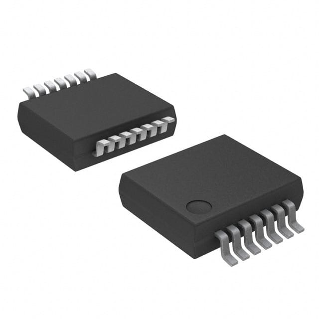
Voir les spécifications pour les détails du produit.

74HC4002DB,112
Basic Information Overview
- Category: Integrated Circuit (IC)
- Use: Logic Gate
- Characteristics: Dual 4-input NOR gate
- Package: SOIC (Small Outline Integrated Circuit)
- Essence: High-speed CMOS technology
- Packaging/Quantity: Tape and Reel, 2500 units per reel
Specifications
- Supply Voltage Range: 2.0V to 6.0V
- Input Voltage Range: -0.5V to VCC + 0.5V
- Output Voltage Range: -0.5V to VCC + 0.5V
- Operating Temperature Range: -40°C to +125°C
- Propagation Delay: 10ns (typical)
Detailed Pin Configuration
The 74HC4002DB,112 has a total of 14 pins. The pin configuration is as follows:
- Input A1
- Input B1
- Output Y1
- Ground (GND)
- Input A2
- Input B2
- Output Y2
- VCC (Supply Voltage)
- Input C1
- Input D1
- Output Z1
- Input C2
- Input D2
- Output Z2
Functional Features
- Dual 4-input NOR gate functionality
- High-speed operation due to CMOS technology
- Wide supply voltage range for flexibility in various applications
- Low power consumption
- Schmitt-trigger action on all inputs allows for noisy input environments
Advantages and Disadvantages
Advantages: - High-speed operation enables efficient data processing - Wide supply voltage range allows for compatibility with different systems - Low power consumption reduces energy usage - Schmitt-trigger action ensures reliable operation in noisy environments
Disadvantages: - Limited to NOR gate functionality, may not be suitable for all logic operations - Requires careful handling due to sensitivity to electrostatic discharge (ESD)
Working Principles
The 74HC4002DB,112 is based on high-speed CMOS technology. It consists of two independent 4-input NOR gates. The inputs are internally connected to Schmitt-trigger circuits, providing noise immunity and allowing reliable operation even in the presence of signal fluctuations. The outputs are capable of driving standard TTL or CMOS loads.
Detailed Application Field Plans
The 74HC4002DB,112 can be used in various applications that require logical operations. Some potential application fields include: - Digital systems design - Data processing units - Communication systems - Industrial automation - Consumer electronics
Detailed and Complete Alternative Models
- 74HC02: Quad 2-input NOR gate
- 74HCT02: Quad 2-input NOR gate with Schmitt-trigger inputs
- CD4001: Quad 2-input NOR gate
- CD4002: Dual 4-input NOR gate
These alternative models offer similar functionality and can be considered as replacements for the 74HC4002DB,112 depending on specific requirements.
Word count: 346 words
Énumérez 10 questions et réponses courantes liées à l'application de 74HC4002DB,112 dans les solutions techniques
Sure! Here are 10 common questions and answers related to the application of 74HC4002DB,112 in technical solutions:
Q: What is the 74HC4002DB,112? A: The 74HC4002DB,112 is a quad 2-input NOR gate integrated circuit (IC) that can be used in various digital logic applications.
Q: What is the operating voltage range for the 74HC4002DB,112? A: The operating voltage range for the 74HC4002DB,112 is typically between 2V and 6V.
Q: How many inputs does the 74HC4002DB,112 have? A: The 74HC4002DB,112 has four inputs, with two inputs per NOR gate.
Q: What is the maximum output current of the 74HC4002DB,112? A: The maximum output current of the 74HC4002DB,112 is typically around 5.2mA.
Q: Can the 74HC4002DB,112 be used in both CMOS and TTL logic systems? A: Yes, the 74HC4002DB,112 is compatible with both CMOS and TTL logic systems.
Q: What is the propagation delay of the 74HC4002DB,112? A: The propagation delay of the 74HC4002DB,112 is typically around 15ns.
Q: Can the 74HC4002DB,112 be used as an AND gate? A: No, the 74HC4002DB,112 is specifically designed as a NOR gate and cannot function as an AND gate.
Q: What is the power supply voltage required for the 74HC4002DB,112? A: The power supply voltage required for the 74HC4002DB,112 is typically between 2V and 6V.
Q: Can the 74HC4002DB,112 be used in high-speed applications? A: Yes, the 74HC4002DB,112 is suitable for high-speed applications due to its low propagation delay.
Q: What is the package type of the 74HC4002DB,112? A: The 74HC4002DB,112 is available in a standard SOIC-14 package.
Please note that the answers provided here are general and may vary depending on specific datasheet specifications or application requirements.

