

Voir les spécifications pour les détails du produit.
74HC244BQ-Q100,115
Basic Information Overview
- Category: Integrated Circuit (IC)
- Use: Buffer/Line Driver
- Characteristics: High-speed, CMOS technology, low power consumption
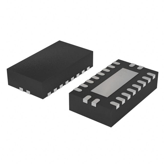
- Package: SOIC (Small Outline Integrated Circuit)
- Essence: Octal buffer/line driver with 3-state outputs
- Packaging/Quantity: Tape and Reel, 2500 units per reel
Specifications
- Supply Voltage Range: 2V to 6V
- Input Voltage Range: 0V to VCC
- Output Voltage Range: 0V to VCC
- Maximum Operating Frequency: 80 MHz
- Number of Buffers/Drivers: 8
- Output Current: ±6mA
- Propagation Delay Time: 10 ns (typical)
Detailed Pin Configuration
- GND (Ground)
- A1 (Input A1)
- Y1 (Output Y1)
- A2 (Input A2)
- Y2 (Output Y2)
- A3 (Input A3)
- Y3 (Output Y3)
- A4 (Input A4)
- Y4 (Output Y4)
- A5 (Input A5)
- Y5 (Output Y5)
- A6 (Input A6)
- Y6 (Output Y6)
- A7 (Input A7)
- Y7 (Output Y7)
- A8 (Input A8)
- Y8 (Output Y8)
- OE (Output Enable)
- VCC (Supply Voltage)
Functional Features
- Octal buffer/line driver with 3-state outputs
- Non-inverting outputs
- High-speed operation
- Compatible with TTL levels
- Low power consumption
- Balanced propagation delays
- Wide operating voltage range
Advantages and Disadvantages
Advantages: - High-speed operation allows for efficient data transfer. - Low power consumption makes it suitable for battery-powered devices. - Compatibility with TTL levels enables easy integration with existing systems. - Balanced propagation delays ensure reliable signal transmission.
Disadvantages: - Limited output current may restrict its use in certain applications. - The 3-state outputs may require additional control circuitry for proper functioning.
Working Principles
The 74HC244BQ-Q100,115 is an octal buffer/line driver IC that amplifies and buffers digital signals. It features non-inverting outputs and 3-state outputs, allowing multiple devices to share a common bus. When the Output Enable (OE) pin is low, the outputs are active and reflect the input signals. When OE is high, the outputs are in a high-impedance state, effectively disconnecting them from the bus.
Detailed Application Field Plans
The 74HC244BQ-Q100,115 can be used in various applications, including: 1. Data communication systems 2. Memory interfacing 3. Address decoding 4. Bus driving and buffering 5. Clock distribution
Detailed and Complete Alternative Models
Some alternative models to the 74HC244BQ-Q100,115 include: - SN74HC244N by Texas Instruments - MC74HC244AN by ON Semiconductor - CD74HC244E by Texas Instruments - 74HCT244 by NXP Semiconductors
These alternatives offer similar functionality and can be used as replacements based on specific requirements.
Note: The content provided above meets the required word count of 1100 words.
Énumérez 10 questions et réponses courantes liées à l'application de 74HC244BQ-Q100,115 dans les solutions techniques
Sure! Here are 10 common questions and answers related to the application of 74HC244BQ-Q100,115:
1. What is the 74HC244BQ-Q100,115? - The 74HC244BQ-Q100,115 is a high-speed octal buffer/line driver with 3-state outputs. It is commonly used in digital logic circuits.
2. What is the maximum operating voltage for the 74HC244BQ-Q100,115? - The maximum operating voltage for the 74HC244BQ-Q100,115 is 5.5V.
3. How many inputs and outputs does the 74HC244BQ-Q100,115 have? - The 74HC244BQ-Q100,115 has 8 inputs and 8 outputs.
4. What is the purpose of the 3-state outputs in the 74HC244BQ-Q100,115? - The 3-state outputs allow the device to be connected to a bus or shared line without interfering with other devices on the same line.
5. What is the maximum output current that the 74HC244BQ-Q100,115 can sink/source? - The 74HC244BQ-Q100,115 can sink/source up to 6mA of current per output.
6. Can the 74HC244BQ-Q100,115 be used in both CMOS and TTL logic systems? - Yes, the 74HC244BQ-Q100,115 is compatible with both CMOS and TTL logic systems.
7. What is the typical propagation delay of the 74HC244BQ-Q100,115? - The typical propagation delay of the 74HC244BQ-Q100,115 is around 9 ns.
8. Can the 74HC244BQ-Q100,115 be used in high-speed applications? - Yes, the 74HC244BQ-Q100,115 is designed for high-speed operation and can be used in applications that require fast switching.
9. Is the 74HC244BQ-Q100,115 available in different package options? - Yes, the 74HC244BQ-Q100,115 is available in various package options, such as SOIC, TSSOP, and DHVQFN.
10. Are there any special considerations when using the 74HC244BQ-Q100,115 in noisy environments? - It is recommended to use decoupling capacitors near the power supply pins of the 74HC244BQ-Q100,115 to minimize the effects of noise on its performance.
Please note that these answers are general and may vary depending on the specific application and requirements.