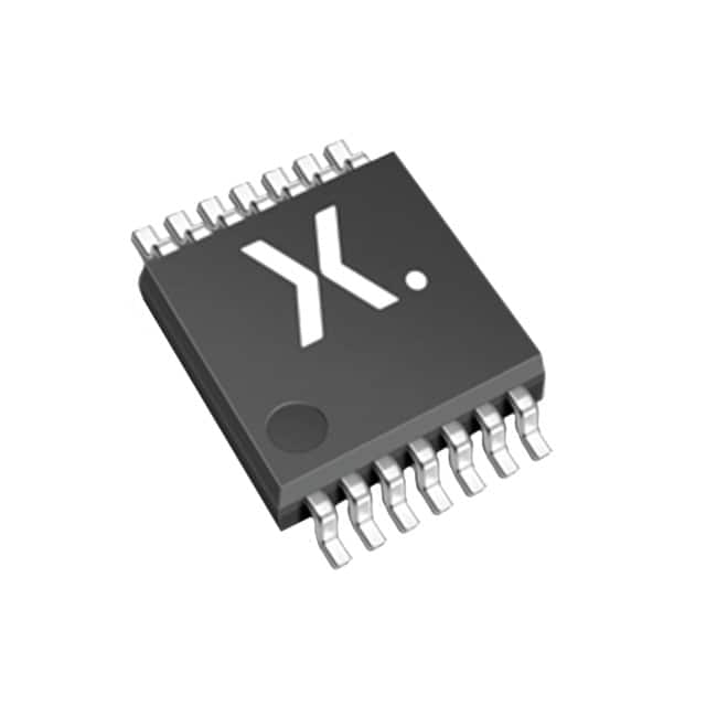
Voir les spécifications pour les détails du produit.

74HC08PW,112
Basic Information Overview
- Category: Integrated Circuit (IC)
- Use: Logic Gate
- Characteristics: Quad 2-input AND gate
- Package: TSSOP-14
- Essence: High-speed CMOS technology
- Packaging/Quantity: Tape and Reel, 2500 units per reel
Specifications
- Supply Voltage Range: 2.0V to 6.0V
- Input Voltage Range: 0V to VCC
- Output Voltage Range: 0V to VCC
- Operating Temperature Range: -40°C to +125°C
- Propagation Delay: 8 ns (typical)
- Maximum Quiescent Current: 4 µA at 5V
Detailed Pin Configuration
The 74HC08PW,112 has a TSSOP-14 package with the following pin configuration:
__    __
   Y1 |1  \__/ 14| VCC
   A1 |2       13| A2
   B1 |3       12| B2
   Y2 |4       11| GND
   A3 |5       10| A4
   B3 |6        9| B4
   Y3 |7        8| Y4
        --------
Functional Features
- Quad 2-input AND gate: The IC consists of four independent AND gates, each having two inputs and one output.
- High-speed operation: Utilizes high-speed CMOS technology, allowing for fast switching times and low power consumption.
- Wide voltage range: Can operate within a supply voltage range of 2.0V to 6.0V, making it compatible with various systems.
- Low quiescent current: Consumes only 4 µA of current at 5V, ensuring energy efficiency.
Advantages and Disadvantages
Advantages: - Compact package: The TSSOP-14 package offers a small footprint, making it suitable for space-constrained applications. - Versatile: Can be used in a wide range of digital logic applications. - High-speed operation: Enables efficient processing of logic signals.
Disadvantages: - Limited number of gates: Contains only four AND gates, which may not be sufficient for complex systems requiring more logic functions. - Sensitivity to voltage fluctuations: The IC may exhibit unpredictable behavior if the supply voltage falls outside the specified range.
Working Principles
The 74HC08PW,112 operates based on the principles of Boolean logic. Each of the four independent AND gates within the IC follows the truth table for an AND gate, where the output is high (logic 1) only when both inputs are high. The internal circuitry utilizes CMOS technology to achieve high-speed operation and low power consumption.
Detailed Application Field Plans
The 74HC08PW,112 finds applications in various fields, including: 1. Digital electronics: Used in the design and implementation of digital circuits, such as arithmetic units, multiplexers, and memory systems. 2. Microcontrollers: Employed in microcontroller-based systems to perform logical operations and control external devices. 3. Communication systems: Integrated into communication protocols and interfaces to handle signal routing and data processing.
Detailed and Complete Alternative Models
Some alternative models that offer similar functionality to the 74HC08PW,112 include: - SN74HC08N: DIP-14 package, compatible with 74HC series logic gates. - CD4081BE: DIP-14 package, quad 2-input AND gate from the CD4000 series. - MC14008B: SOIC-14 package, quad 2-input AND gate from the MC14000B series.
These alternative models can be considered based on specific requirements, availability, and compatibility with existing systems.
Word count: 408 words
Énumérez 10 questions et réponses courantes liées à l'application de 74HC08PW,112 dans les solutions techniques
Sure! Here are 10 common questions and answers related to the application of 74HC08PW,112 in technical solutions:
Q: What is the 74HC08PW,112? A: The 74HC08PW,112 is a quad 2-input AND gate integrated circuit (IC) that is commonly used in digital logic circuits.
Q: What is the operating voltage range for the 74HC08PW,112? A: The operating voltage range for the 74HC08PW,112 is typically between 2V and 6V.
Q: How many inputs does the 74HC08PW,112 have? A: The 74HC08PW,112 has four inputs, allowing you to connect up to four different signals.
Q: What is the output voltage level of the 74HC08PW,112? A: The output voltage level of the 74HC08PW,112 is typically equal to the supply voltage.
Q: Can the 74HC08PW,112 be used with both TTL and CMOS logic levels? A: Yes, the 74HC08PW,112 is compatible with both TTL and CMOS logic levels, making it versatile for various applications.
Q: What is the maximum frequency at which the 74HC08PW,112 can operate? A: The 74HC08PW,112 can typically operate at frequencies up to 50 MHz.
Q: Can the 74HC08PW,112 be used as a buffer or amplifier? A: No, the 74HC08PW,112 is specifically designed as an AND gate and is not suitable for use as a buffer or amplifier.
Q: What is the power consumption of the 74HC08PW,112? A: The power consumption of the 74HC08PW,112 is typically low, making it suitable for battery-powered applications.
Q: Can the 74HC08PW,112 be used in both digital and analog circuits? A: No, the 74HC08PW,112 is designed for digital logic applications and is not suitable for use in analog circuits.
Q: Are there any specific precautions to consider when using the 74HC08PW,112? A: It is important to ensure that the supply voltage does not exceed the specified range, and proper decoupling capacitors should be used to minimize noise and voltage spikes.
Please note that these answers are general and may vary depending on the specific datasheet and manufacturer's recommendations for the 74HC08PW,112.

